Consequences of Insufficient Component Spacing in PCB Design: A Case Study
27 Mar, 2024
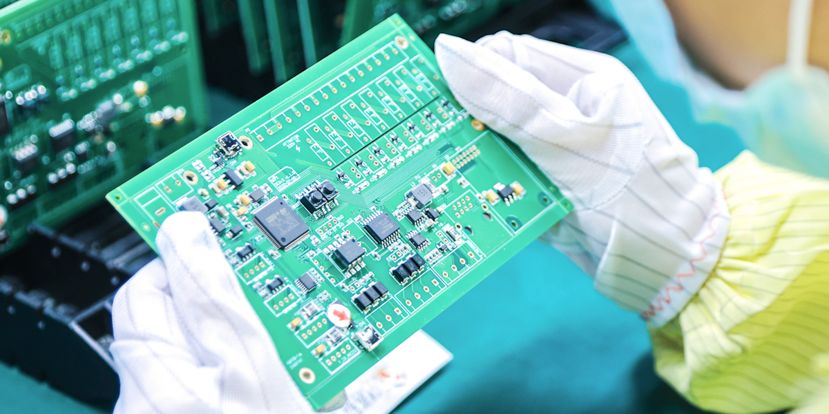
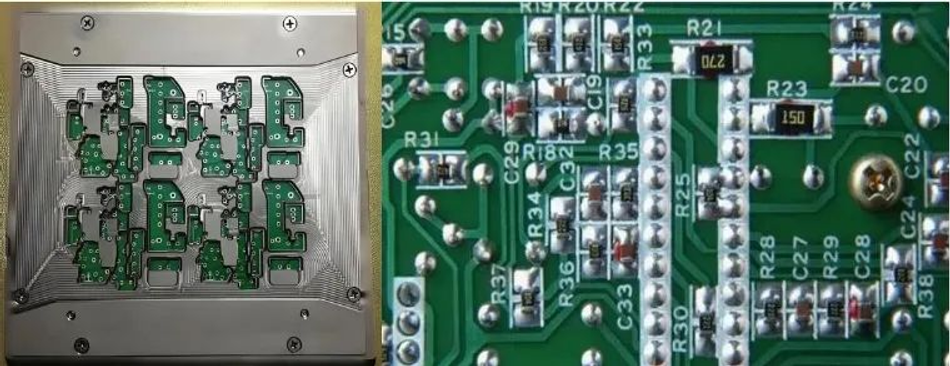
PCB Assembly SMT Inspection
Adequate component spacing is typically not high on the PCB designer's list of priorities, but oversights can be frustrating and could demand substantial re-work. Here we look at an example, give general guidelines and look at how tools can be used to educate designers and save time.
It is easy to take for granted actual scales when zoomed in on modern high-res flat-screens, but in reality, the surfaces of PCB boards are not two-dimensional with precisely defined edges. The layers of copper, solder mask, silkscreen and non-planar surface finishes are raised and allowing for solder mask expansion and dams can reduce space between elements even further.
Allowing for sufficient component clearances is something PCB designers know all about, but many inexperienced and experienced designers still end up digging their own graves to avoid a little bit of extra rerouting.
As careful engineer Xiao Peng learned, the perfect layout depends not only on one’s experience but also on one’s toolbox. Various tools are freely available to provide a systematic and automated approach to detecting such issues and improving the layout overall.
Xiao Peng is a PCB layout engineer with over a decade of industrial experience under his belt from layout to production. But his recent experience caused him to doubt his abilities.
As per his standard workflow, Xiao Peng’s pre-production checks consist of meticulous design review covering signal integrity, functionality and performance, design for manufacture (DFM) and design for assembly (DFA). However, for this particular batch undergoing wave soldering, the incidence of cold solder joints and insufficient through-hole barrel fill defects was unusually high. Consequently, the batch failed to meet IPC Class 2 standards.
IPC Class 2 standards define strict requirements for solder joints. For through-hole joints, the barrel must have a minimum solder fill ratio of 75%, with 25% sinking allowed.
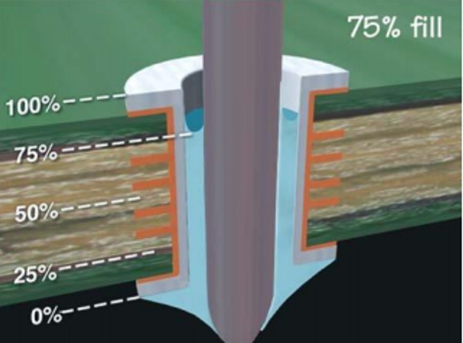
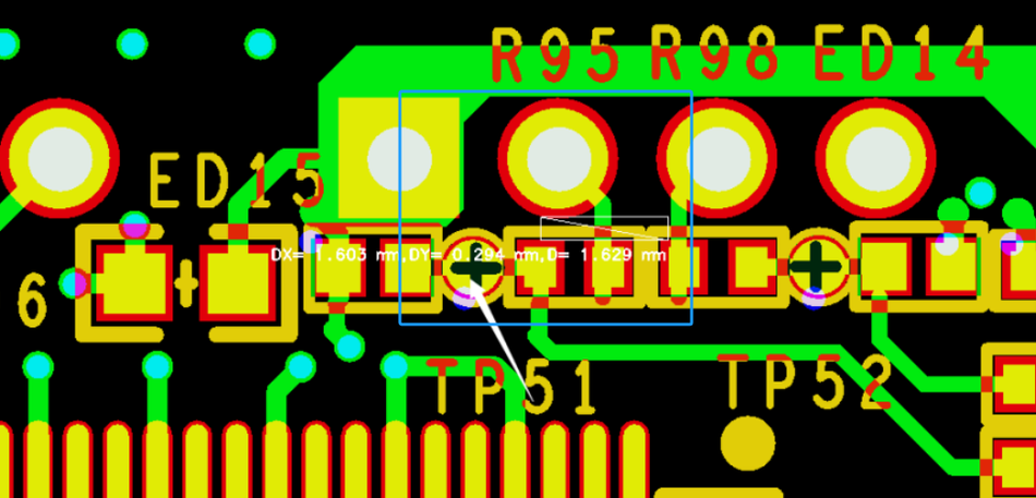
Xiao Peng suspected that the nearby surface mount resistor could be the culprit and upon inspection, found that the distance between the pads was only 0.2mm. This spacing was more than enough for solder mask dams to form and prevent solder bridges, however, the effect on the through-hole joint was not clear. After consulting the assembly technicians, it was found that the board was suffering from shadowing effects.
PCB shadowing is the phenomenon whereby taller parts cast shadows on other lower neighboring parts which can have consequences on soldering, thermal management and signal integrity. For wave soldering, the nearby components can physically block molten solder from reaching certain areas of the PCB, in this case, the through-hole barrels.
To remedy the issue, the technicians recommended a clearance of 3mm to mitigate the effects of shadowing, and even more for taller components.
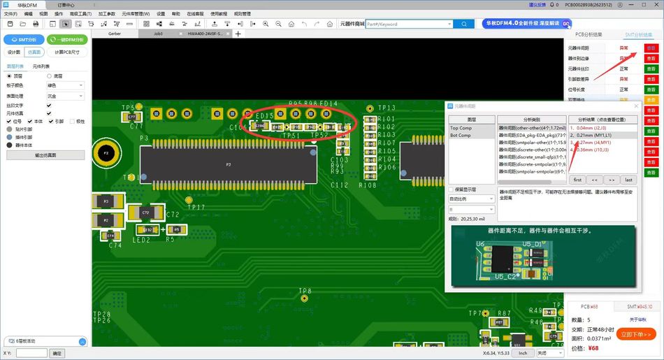
At the same time, HQDFM, the PCB design analysis software from HQ Electronics was recommended to Xiao Peng, which claims to be able to detect PCB shadowing issues and many other DFM issues. HQDFM indeed highlighted the spacing issue among other errors. After following the suggestions, the new design effectively eliminated cold solder and barrel filling defects.
As Xiao Peng discovered, even the most experienced engineers could do with extra assistance here and then. Unlike in China, where engineers can freely contact their manufacturers and expertise is common, overseas designers outsourcing overseas will have time differences, language barriers and limited resources to contend with.
“I am deeply aware of the close relationship between quality and design. A good design can not only improve product performance and quality but also reduce production costs and difficulty. Inbuilt DRCs are one way of detecting issues, but they are often limited and are based on black-and-white values you have to feed in yourself. HQDFM on the other hand is powerful, informative and explicit in its goals to reduce manufacturing issues and improve reliability even if you don’t use HQ for production.
I especially liked the fact that HQDFM is free yet powerful. HQDFM looks at everything from bare board spacings to component heights and the impact on wave soldering and gives specific recommendations and figures. There aren’t many tools outside of EDA programs that can be considered essential in the designer’s toolbox but HQDFM is one of them and I will be using it extensively from now on.” - Xiao Peng
Common spacing pitfalls and guidelines
Knowing what to look out for and the potential impact is the first step for PCB designers to improve their DFM evaluation skills which can then be incorporated at the earliest stage of design. The second is the ability to quickly detect issues, which can be accomplished with tools like HQDFM. HQDFM helps to achieve both of these goals through education and detection. Some of the component spacing issues covered by HQDFM include:
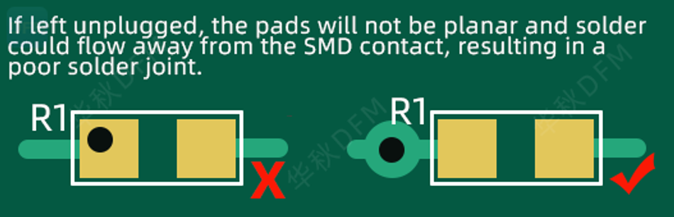
Through-hole to Surface Mount Pad Spacing
In Xiao Peng’s case, the close proximity of the through-hole and surface mount pads resulted in the through-hole being inadequately filled during wave soldering. For reflow soldering, insufficient spacing between through-holes, opened vias, test points, metallic mounting holes, and surface mount pads can result in solder being pulled away from the surface mount pad, resulting in poor wetting and making solder defects such as tombstones more likely.
If spacing is limited, consider putting vias on pads, but these should be plugged and capped to prevent solder from leaking through the via. Be aware that via plugging and capping require specialist machinery and come at an additional cost.
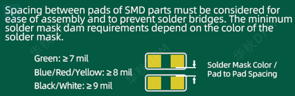
Solder Mask Dams
Any two objects that are so close together that they do not leave room for solder mask dams are at risk of solder bridges. Solder mask, or also accurately named solder resist, is your best friend in both SMT and wave soldering as it helps to prevent solder from building up where it is not wanted. For fine-pitch components, especially chips with underside pads, dams can be a lifesaver. For a single reflow, you can probably get away with suitably sized stencil openings, but when it comes to rework and manual soldering, the lack of dams will require greater skill and patienceharder.
Pro-tip: most PCB manufacturers have their own solder mask expansion values and will not necessarily follow the lengths in your Gerber files. So a more accurate way of determining if the spacing is large enough for dams to form is to follow pad-to-pad (copper to copper) spacing from manufacturers. Also, remember that values typically vary according to solder mask color. If color is not important, sticking with regular green will produce the best results. If you need to push the limits further, use ENIG plating for a planar pad surface.
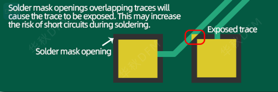
Solder Mask Opening to Trace Spacing
Traces positioned too close to pads may inadvertently be exposed as a result of solder mask expansion and be at risk of shorting. Ensure traces are sufficiently covered to protect the trace and ensure it remains sealed by the solder mask film.
Through-hole Spacing
Whether soldered manually or automated, through-hole leads need to be reachable, be it by a soldering iron, wave, lead clippers, etc. Therefore the area around them must be void of obstacles such as tall components and other leads. Insufficient adjacent and overhead clearance could result in tricky soldering positions and accidental melting of other components or oneself.
Lower on the ground, leads of adjacent through-hole parts should be far enough to prevent solder bridges. For through-hole parts, solder mask dams are a must, which can be achieved by reducing the diameter of pads or shaving material off the edges.
Wave Soldering Considerations
Wave soldering’s main advantage is the ability to solder through-hole parts in volume but comes at a cost. Layout engineers have a whole host of extra restrictions to compete with, limiting placement options and possibly ruling out higher-density designs. In addition to leaving extra space between parts, engineers have to constantly consider the direction of the incoming wave, shadowing effects and the use of glue or fixtures for mixed assembly.
As we have explored, the consequences of something as simple as component spacing can have grave consequences, but as the DFM mantra goes, it’s better to be safe than sorry. Experienced layout engineers and beginners should make it part of their workflow to pay special attention to spacings and use tools such as HQDFM to accelerate mundane tasks and act as a safety net.
HQDFM is a free PCB design analysis software covering bare board and populated PCB analysis. With over 200 inspection items under 30 DFM and DFA categories including trace, solder mask and drill clearances, pads dimensions, shorts/opens, drill hole sizes and solder mask dams. HQDFM also provides tools for the designing and manufacturing PCBs including an impedance calculator, panelization tool, footprint, BOM and centroid file checker.
Transform your workflow and swiftly integrate DFM methodologies into your product development with the HQDFM desktop suite from HQ Electronics (NextPCB).