EMI Shielding: Protecting Electronic Devices in a Noisy World

20 Apr, 2024
Discover the science behind EMI shielding and its crucial role in ensuring the reliability and performance of electronic devices across various industries.
Introduction
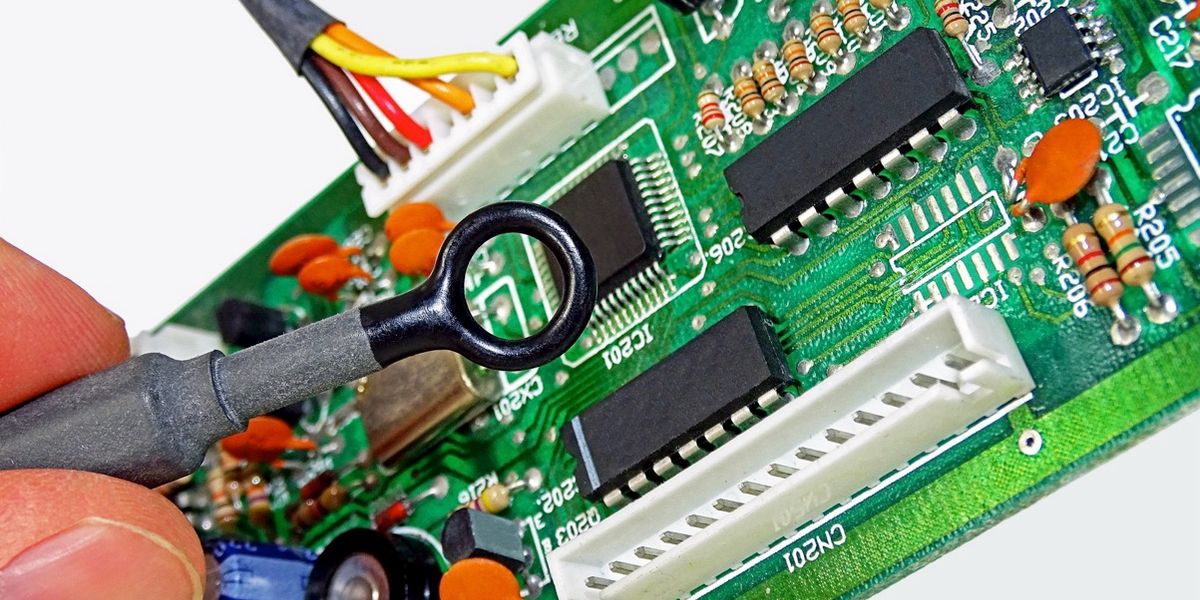
Electronic devices are everywhere, ranging from smartphones in our pockets to complex systems in the aerospace and medical industries. These devices are vulnerable to electromagnetic interference (EMI), which can compromise their performance and reliability.
EMI shielding is a crucial element in electronic device design, protecting sensitive components from disruptive electromagnetic signals. By effectively implementing EMI shielding techniques, engineers can ensure the proper functioning and longevity of electronic systems across various industries. This article explores the science behind EMI shielding and its critical role in maintaining the integrity of electronic devices in today's interconnected world.
Understanding the Fundamentals of EMI
Electromagnetic Interference (EMI) is a phenomenon where unwanted electromagnetic energy disrupts the normal operation of electronic devices or systems. It is the coupling of signals from two or more systems that creates disturbance and causes distortion in the output signals.
EMI sources are mainly of two types i.e.
Natural Sources - Lightning strikes, Cosmic microwave background and solar flares
Man-made - Power lines, motors, cellular networks and other electronic measurement and control devices.
The effects of EMI range from minor disturbances to complete system failure, depending on the intensity and frequency of the interference.
EMI manifests in two main forms:
Conducted EMI - Propagates through physical connections like cables and wires
Radiated EMI - Travels through the air as electromagnetic waves
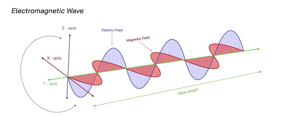
The propagation of electromagnetic waves follows Maxwell's equations, which describe the relationship between electric and magnetic fields. In free space, the wave equation for electric field E is:

where 'c' is the speed of light in vacuum.
Role of Coupling Mechanisms in EMI
Coupling mechanisms, such as capacitive and inductive coupling, dictate how EMI affects electronic devices. There are two main types of coupling mechanisms:
Capacitive Coupling
Capacitive coupling occurs when the electric field of the interference source induces a voltage in the victim circuit. Typically, it happens when two conductors are present in a very close proximity having a distance of less than a wavelength between them. Due to such a tiny space, it creates a parasitic capacitance, allowing charge to be stored and transferred through charge differentials created by the electric fields. This parasitic capacitance distorts the original signals.
Inductive Coupling
Inductive coupling happens when the magnetic field induces a current. It is similar to capacitive coupling but the crosstalk occurs due to current flow through electromagnetic induction. It typically happens when the current in one of the conductors oscillates or changes frequently, leading to signal integrity issues, like crosstalk and ground bounce.EMI Issues in Industries
EMI issues are common in various industries:
Automotive - EMI from high-voltage ignition systems and electric motors can affect sensitive electronic control units (ECUs) and in-vehicle infotainment systems
Medical - EMI from medical equipment like MRI machines and electrosurgical units can interfere with the functioning of pacemakers and other implantable devices
Aerospace - EMI from radar systems and avionics can disrupt the operation of navigation and communication equipment, potentially compromising flight safety
In digital circuits, EMI can cause bit errors, clock jitter, and false triggering of logic gates. Analog circuits may experience noise, distortion, and unwanted oscillations, leading to degraded signal quality and reduced dynamic range.
Types of EMI and Their Characteristics
Electromagnetic interference (EMI) can be classified into three main types based on how it propagates and affects electronic devices and systems. The following table summarizes the characteristics and effects of different types of EMI:
Type of EMI | Characteristics | Effects |
Conducted EMI |
|
|
Radiated EMI |
|
|
Coupled EMI |
|
|
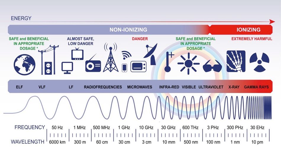
Frequency Spectrum and EMI Susceptibility
The electromagnetic frequency spectrum is a continuous range of all possible frequencies, spanning from extremely low frequencies (ELF) as low as 1 Hertz to gamma rays with frequencies of more than 1025. Different portions of the spectrum can affect electronic devices and systems differently, leading to varying levels of EMI susceptibility.
At lower frequencies, such as the ELF range (3 Hz to 30 Hz) and the Very Low frequency (VLF) range (3 kHz to 30 kHz), EMI is primarily caused by power line emissions and natural phenomena like lightning. These frequencies can induce currents in long conductors, causing conducted EMI issues.
As the frequency increases, the wavelength of the electromagnetic waves decreases, making it easier to propagate through space and cause radiated EMI. In the high frequency (HF) range (3 MHz to 30 MHz) and the very high frequency (VHF) range (30 MHz to 300 MHz), EMI can be generated by sources such as radio transmitters, mobile phones, and high-speed digital circuits, leading to signal integrity issues and performance degradation in nearby electronic devices.
In the ultra-high frequency (UHF) range (300 MHz to 3 GHz) and beyond, EMI becomes more prevalent due to the increasing use of wireless communication systems, radar, and microwave devices. The shorter wavelengths at these frequencies allow for more efficient coupling of electromagnetic energy into electronic devices and systems, resulting in increased susceptibility to radiated EMI and potential issues like signal distortion, data corruption, and system malfunctions.
The following visual representation illustrates the electromagnetic frequency spectrum and the relative EMI susceptibility levels across different frequency ranges:
What is EMI Shielding?
Since electromagnetic interference can easily disrupt signals, it can create unwanted disturbances and integrity issues in electronic systems. That’s where EMI shielding comes in. EMI shielding in electronic devices and equipment involves using manufacturing techniques and materials to safeguard signals from external electromagnetic interference and prevent generated signals from disturbing surrounding components.
The shield creates a barrier to prevent leakage of strong electromagnetic fields that could disrupt sensitive devices and signals. Typically, the shielding is installed to
Isolate the source of the electromagnetic field
Enclose the device needing protection.
Principles and Mechanisms of EMI Shielding
EMI shielding is based on the fundamental principles of electromagnetic field theory and the interaction of electromagnetic waves with conductive materials. Its primary goal is to reduce the intensity of electromagnetic fields that can cause interference in electronic devices and systems by creating a barrier that reflects, absorbs, or redirects the electromagnetic energy away from the protected device or system.
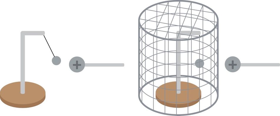
Faraday Cages
Faraday cages are one of the most effective methods of EMI shielding. A Faraday cage is an enclosure made of conductive material that acts as a shield against electromagnetic fields by redistributing the charges on its surface in response to an external electromagnetic field, creating a counteracting field that cancels out the original field inside the enclosure. This principle is based on Gauss's law, which states that the net electric flux through any closed surface is proportional to the net electric charge enclosed within that surface.
EMI Shielding Mechanisms
The effectiveness of EMI shielding depends on three main mechanisms:
Reflection
When electromagnetic waves encounter a conductive surface and are reflected back towards the source. The reflection loss (R) can be calculated using the following equation:

where 'σr' is the relative conductivity of the shielding material, 'f' is the frequency of the electromagnetic wave, and 'μr' is the relative magnetic permeability of the shielding material.
Higher conductivity in the material yields better shielding characteristics. However, the downside of the reflection mechanism is that if any discontinuity in the shielding enclosure is larger than the wavelength, the reflection mechanism doesn’t remain as effective. Hence, the mechanism typically fails for high-frequency electromagnetic waves.
Absorption
When electromagnetic energy is dissipated as heat within the shielding material. The absorption loss (A) can be calculated using the following equation:

Absorption is a secondary shielding mechanism that focuses on the magnetic component of the EMI. Such shielding materials feature electric and magnetic dipoles having a high dielectric constant and magnetic permeability.
As external magnetic lines come across the material, they are cut down by the material’s magnetic properties while the conductive components of the enclosure absorb the electric lines of field. However, these components don’t always have high conductivity, so they are less effective in absorbing the electric component of the EMI.
Multiple Reflections
When electromagnetic waves are reflected back and forth within the shielding material, leading to further attenuation of the field strength. The multiple reflection loss (M) can be calculated using the following equation:

The total shielding effectiveness (SE) is the sum of the reflection loss, absorption loss, and multiple reflection loss:

The electrical and magnetic properties of shielding materials play a crucial role in determining their effectiveness.
Materials with high electrical conductivity, such as copper and aluminum, are excellent at reflecting electromagnetic waves,
Materials with high magnetic permeability, such as mu-metal and permalloy, are effective at absorbing electromagnetic energy.
The skin depth of the shielding material also affects its performance, as it determines the depth at which the electromagnetic field can penetrate the material. A smaller skin depth results in better shielding effectiveness, especially at higher frequencies.
Shielding Materials and Their Properties
Various materials are used for EMI shielding, each with unique properties and characteristics that make them suitable for different applications. The most common categories of shielding materials and their properties are discussed in the following table:
Material Category | Examples | Electrical Conductivity | Magnetic Properties | Shielding Effectiveness | Density | Flexibility |
Metals | Copper, Aluminum, Steel | High | Ferromagnetic (steel) | High | High | Low |
Conductive Polymers | PANI, PPy | Moderate | Non-magnetic | Moderate | Low | High |
Composites | Carbon-filled, Metal-filled | Moderate to High | Depends on filler | Moderate to High | Low to Moderate | Moderate |
The choice of shielding material depends on various factors, such as the frequency range of the electromagnetic interference, the required level of shielding effectiveness, the weight and size constraints of the application, and the environmental conditions in which the shielding will be used.
Recommended Reading: NANOWEB - A Revolutionary Transparent Conductive Thin Film
EMI Shielding Design Considerations and Best Practices
Designing effective EMI shielding for electronic devices requires careful consideration of various factors to ensure optimal shielding performance. Key factors include:
Shielding Geometry and Material Selection
Ideal shielding geometry - Completely enclosed, seamless conductor surrounding the electronic device or system.
Apertures - Keep as small as possible (< 1/20th of the wavelength of the highest frequency of concern), use conductive gaskets, meshes, or filters to maintain electrical continuity, and locate away from high-frequency noise sources and sensitive components.
Seams and joints Minimize seams - use continuous welding, brazing, or soldering for low-impedance, electrically continuous joints, employ conductive gaskets, and orient seams perpendicular to the electromagnetic field.
Accurate shielding geometry can be achieved by using advanced manufacturing techniques such as 3D printing, allowing the development of complex and intricate shielding enclosures for novel electronic systems.
Likewise, when it comes to material selection, here are a few important considerations:
Low-frequency EMI (< 1 MHz) - Use materials with high magnetic permeability, such as mu-metal or permalloy.
High-frequency EMI (> 1 MHz) - Use materials with high electrical conductivity, such as copper or aluminum.
Harsh environments - Select materials with appropriate thermal, chemical, and mechanical properties.
Gaskets and Seals
Gaskets and seals are essential components in EMI shielding design, ensuring electrical continuity and preventing leakage at interfaces and seams. These components maintain the integrity of the shielding enclosure and minimize the impact of apertures and gaps on shielding effectiveness.
Gaskets, compressible materials used to fill gaps and create continuous electrical contact between mating surfaces, come in various forms:
Conductive elastomers - Made from elastomeric materials (silicone or fluorosilicone) offering good compression-deflection characteristics and conformity to irregular surfaces.
Knitted wire mesh - Made from knitted wire mesh (monel, aluminum, or stainless steel), providing high shielding effectiveness and handling high temperatures and mechanical stress.
Fingerstock - Consisting of multiple thin, flexible metal strips in a comb-like pattern, offering low contact resistance and accommodating relative motion between surfaces.
Recommended Reading: 3D Printed Rubber: What's Possible and What Isn't
Conductive AdhesivesConductive adhesives, used to bond shielding components together and provide electrical continuity across joints, are available in various forms:
Epoxy-based adhesives - Conductive filler (silver or nickel) dispersed in an epoxy resin matrix, offering good adhesion, low contact resistance, and room temperature or heat curing.
Silicone-based adhesives - Conductive fillers in a silicone rubber matrix, provide good flexibility, temperature stability, and adhesion to various substrates.
Acrylic-based adhesives - Conductive fillers combined with an acrylic resin matrix, offer good adhesion, conductivity, and application as a thin film or tape.
Real-world examples of gaskets and adhesives in EMI shielding solutions:
Smartphone shielding: Conductive elastomer gaskets sealing gaps between metal housing and display or battery cover, preventing EMI leakage from internal components.
Automotive electronics: Knitted wire mesh gaskets in electronic control units (ECUs) and automotive electronic modules, providing EMI shielding and reliable operation in harsh environments.
Medical devices: Conductive epoxy adhesives bonding shielding enclosures and creating a continuous electrical ground in MRI scanners and pacemakers, protecting them from EMI.
Aerospace applications: Fingerstock gaskets in avionics equipment and satellite systems, providing EMI shielding and accommodating relative motion between surfaces due to thermal expansion or vibration.
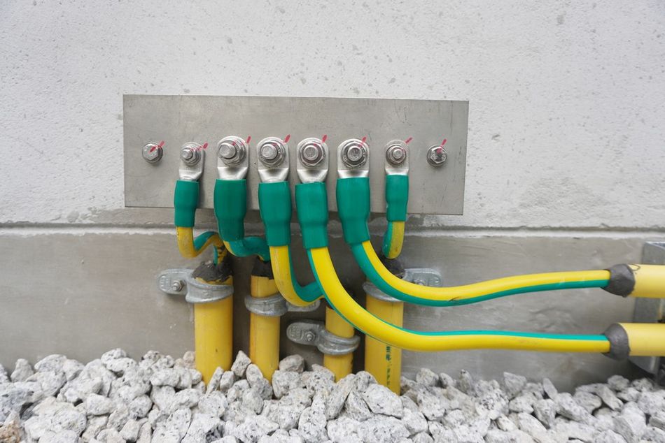
Grounding, Bonding, and Termination Techniques
Proper grounding, bonding, and termination are essential for effective EMI shielding design, ensuring that electromagnetic energy is diverted away from sensitive components.
Grounding connects shielding components to a common reference point (earth ground)
Bonding creates a continuous, low-impedance path between components.
Various techniques, including direct metal-to-metal contact, conductive gaskets, grounding straps, and shielded connectors, are used depending on specific application requirements.
Best practices involve minimizing impedance through short, wide, and multiple connections, preparing mating surfaces for good electrical contact, and selecting appropriate termination techniques.
Factors such as frequency range of interference dictate the choice of grounding and bonding methods, with considerations like wider and thinner conductors for higher frequencies. Regular inspection and maintenance are crucial for long-term effectiveness, especially in harsh environments.
Challenges and Future Directions in EMI Shielding
While EMI shielding is an essential aspect of electronic device design, it presents several challenges and limitations that must be considered and addressed to ensure optimal performance and cost-effectiveness. Some of the main challenges associated with EMI shielding include:
Weight
Shielding materials, particularly metals, can add significant weight to electronic devices, which is a critical concern in applications such as aerospace and portable electronics. Lightweight shielding materials, such as conductive polymers and composites, have been developed to address this challenge, but they often come with trade-offs in terms of shielding effectiveness and cost.
Cost
Implementing effective EMI shielding can be expensive, especially for complex devices with multiple components and intricate geometries. The cost of shielding materials, fabrication processes, and testing can add up quickly, making it challenging to balance shielding performance with economic viability.
Manufacturing Complexity
Designing and manufacturing EMI shielding solutions can be complex, particularly for devices with tight tolerances, intricate shapes, and multiple interfaces. Ensuring proper fit, alignment, and continuity of shielding components requires careful design, precise manufacturing, and rigorous quality control, which can increase production time and cost.
Thermal Management
EMI shielding materials can impact the thermal performance of electronic devices by affecting heat dissipation and airflow. This is particularly challenging in high-power devices where effective thermal management is critical for reliability and longevity. Designers must carefully balance the need for EMI shielding with the thermal requirements of the device, often requiring the use of specialized materials or cooling techniques.
Emerging Technologies that Tackle Challenges with EMI Shielding
Emerging technologies and materials offer promising solutions to some of the challenges associated with EMI shielding. For example:
Nanomaterials
Nanostructured materials, such as carbon nanotubes and graphene, have exceptional electrical and thermal properties that make them attractive for EMI shielding applications. These materials can be incorporated into composites or coatings to provide lightweight, flexible, and highly effective shielding solutions.
Metamaterials
Metamaterials are artificially engineered structures that can manipulate electromagnetic waves in ways not found in natural materials. They have the potential to create ultra-thin, frequency-selective shielding surfaces that can be tuned to specific applications, reducing weight and cost while maintaining high shielding effectiveness.
3D printing
Additive manufacturing techniques, such as 3D printing, enable the fabrication of complex shielding geometries that would be difficult or impossible to produce using traditional manufacturing methods. This can lead to more efficient and cost-effective shielding solutions, particularly for low-volume or custom applications.
Smart Materials:
Materials that can adapt their properties in response to external stimuli, such as temperature or electric fields, could enable the development of active EMI shielding solutions. These materials could dynamically adjust their shielding performance based on the changing electromagnetic environment, providing optimal protection while minimizing weight and cost.
Conclusion
This comprehensive guide has explored the fundamental concepts, principles, and techniques of EMI shielding in the engineering field. We have discussed the importance of shielding materials, the principles and mechanisms of EMI shielding, and the critical role of gaskets, seals, conductive adhesives, and proper grounding and bonding techniques in ensuring the effectiveness of shielding solutions.
The challenges and limitations associated with EMI shielding, such as weight, cost, and manufacturing complexity, were also addressed, highlighting the need for innovative solutions and emerging technologies to overcome these obstacles.
Frequently Asked Questions (FAQs)
What is the difference between EMI shielding and EMC?
EMI shielding focuses on preventing electromagnetic interference from affecting electronic device performance, while EMC (electromagnetic compatibility) encompasses both EMI shielding and other techniques to ensure electronic devices operate correctly in their intended electromagnetic environment without causing interference to other devices.
How do I select the right shielding material for my application?
Consider factors such as the frequency range of the electromagnetic interference, required shielding effectiveness, weight and size constraints, environmental conditions, and the electrical, magnetic, and mechanical properties of the materials, as well as their cost and availability.
What is the difference between near-field and far-field shielding?
Near-field shielding attenuates electromagnetic fields close to the source, where electric and magnetic fields are not yet coupled. Far-field shielding attenuates electromagnetic waves that have propagated away from the source. Shielding techniques and materials may differ based on the specific characteristics of the electromagnetic fields involved.
How can I test the effectiveness of my EMI shielding solution?
Methods include shielding effectiveness (SE) measurements, electromagnetic compatibility (EMC) testing, and electromagnetic interference (EMI) testing. SE measurements compare electromagnetic field strength with and without shielding, while EMC and EMI testing assess device operation in its intended electromagnetic environment without causing interference.
Can I use 3D printing to create EMI shielding components?
Yes, 3D printing can create EMI shielding components, particularly for complex geometries or custom applications. Conductive filaments with metal particles or carbon nanotubes can be used, but their performance may not match traditional metal enclosures. Post-processing techniques like electroplating or conductive coating may be necessary for desired shielding effectiveness.
How do I ensure proper grounding and bonding in my EMI shielding design?
Use low-impedance connections (wide, short straps or braids) to minimize inductance and resistance. Prepare and treat mating surfaces for good electrical contact and corrosion prevention. Use appropriate termination techniques (crimping, soldering, welding) for reliable connections. Consider the frequency range and select effective grounding and bonding techniques.
What are some emerging technologies and materials for EMI shielding?
Promising advancements include nanomaterials (carbon nanotubes, graphene) for lightweight, flexible shielding; metamaterials for ultra-thin, frequency-selective surfaces; 3D printing for complex geometries; and smart materials that adapt properties for active EMI shielding solutions that dynamically adjust performance. based on the changing electromagnetic environment.
References
Search for articles and topics on Wevolver
More by Muhammad Sufyan
Meet Sufyan - an accomplished Electronics Engineer and dedicated Educator who teaches at Mohammad Ali Jinnah University in Karachi, Pakistan. With a Master's degree in Electrical Engineering, Sufyan specializes in teaching courses on Microcontrollers, Digital Electronics, and Control Systems. He has...

What is an Open Circuit: A Deep Dive for Engineers
10 minutes read