Microvias: Pioneering the Future of PCB Design and Electronics Miniaturization

15 Mar, 2024
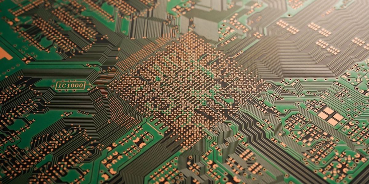
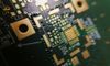
PCB with a green solder mask and high-density interconnects
A microvia connects layers in HDI substrates and PCBs, enabling high input/output density in advanced packages. This article delves into the role and significance of microvias in modern electronics, exploring their impact on device miniaturization and functionality.
Introduction
Microvias represent a crucial innovation in printed circuit board (PCB) design, marking a significant leap toward the miniaturization and enhanced functionality of electronic devices. These minute electrical connections are integral to multilayer PCBs, enabling interlayer connections in increasingly compact electronic assemblies. As the demand for smaller, faster, and more powerful electronic devices grows, microvias have become essential in meeting these stringent requirements.
Their significance in modern electronics cannot be overstated; microvias facilitate developing high-density interconnect (HDI) PCBs, which are crucial for advanced applications ranging from smartphones and tablets to medical devices and aerospace electronics. By allowing for more components to be packed into smaller spaces without compromising performance, microvias contribute to the ongoing evolution of electronic products, pushing the boundaries of what's possible in PCB design and functionality.
The fabrication process of microvias involves advanced materials and processes, including laser drilling, which allows for the precise creation of these small features. The materials chosen for constructing microvias, such as copper for the conductive filling, are selected for their electrical and thermal properties. This ensures the vias can handle the required current loads and dissipate heat effectively. The importance of these technical specifications in PCB design cannot be overstated. The size and depth of microvias influence not only the electrical performance of the PCB but also its thermal management and mechanical stability. Understanding and adhering to these specifications is crucial for engineers and designers aiming to leverage the benefits of microvia technology in their electronic devices.
Understanding Microvias
Microvias are integral to modern printed circuit board (PCB) architecture, especially in high-density interconnect (HDI) technology. These small-diameter holes, typically less than 150 micrometers in diameter, enable electrical connections between different layers of a PCB, supporting the miniaturization of electronic devices and enabling more compact and complex designs. The evolution of via technology, driven by the demand for smaller, more efficient devices, has led to adopting microvias instead of traditional through-hole vias.
Microvias come in three main types: blind microvias, buried, and through-hole. Blind vias connect an outer layer of the PCB to one or more inner layers without penetrating the entire board. Buried vias are contained within the inner layers and are not visible outside. Though through-hole vias are not typically considered microvias due to their larger size, they have been adapted in microvia technology to connect multiple layers from the top to the bottom of the PCB. These different types of microvias offer various characteristics and applications, which are crucial for the design and functionality of modern electronic devices.
The stackup of a PCB, which refers to the arrangement of copper and insulating layers, is crucial in accommodating micro vias. The plating process used in microvias ensures a reliable electrical connection and is essential for maintaining signal integrity and controlling impedance. The small holes drilled for micro vias, typically less than 150 microns in diameter, are strategically placed in the stackup to facilitate interlayer connections. This precise placement is crucial for high-density PCBs, where space is limited, and impedance control is critical for signal performance.[1]
The Technical Specifications of Microvias
The specifications of microvias, including size, depth, diameter, and aspect ratio, play a crucial role in high-density interconnect (HDI) PCB design. Typically, a microvia has a diameter of less than 150 micrometers, with depth varying based on the application and the number of layers it connects within the PCB stackup. The aspect ratio, which is the depth-to-diameter ratio, is particularly important in microvias design as it affects fabrication and performance, especially in stacked microvias.
Fabricating microvias involves advanced materials and processes, such as laser drilling, to ensure precise creation. Materials like copper are chosen for their excellent electrical and thermal properties, which are essential for handling current loads and dissipating heat effectively. These specifications are pivotal in HDI PCB design, directly impacting density, functionality, and overall performance.
In addition to specifications, aspects like stacked microvias, via-in-pad design, PCB layout, and overall PCB fabrication play vital roles. Stacked microvias enhance signal integrity and reduce crosstalk, especially in high-speed applications. Controlling the aspect ratio in stacked microvias is critical for proper plating and reliability. Via-in-pad design, where the microvia is placed directly under a component pad, helps reduce the PCB footprint and improve signal integrity.
Proper PCB layout is essential to ensure that microvias are placed accurately and do not interfere with other components or traces. Additionally, precise lamination processes are necessary to ensure the integrity of the microvias and overall PCB reliability. Understanding and adhering to these specifications and considerations are essential for leveraging the benefits of microvia technology in electronic devices.
Recommended reading: Via in Pad PCB Design
Comparison with Traditional Vias
Microvias and traditional through-hole vias play crucial roles in creating electrical connections between different printed circuit board layers (PCB), but they differ significantly in size, functionality, and application. Traditional through-hole vias penetrate the entire PCB, connecting the top and bottom layers. In contrast, microvias are much smaller in diameter and are used to connect adjacent layers or skip a layer, enabling more complex and compact PCB designs.
One of the primary advantages of microvias is their size. Their smaller diameter allows for more connections within the same PCB area. This is crucial for high-density interconnect (HDI) PCBs where space is limited and functionality is critical. Additionally, microvias can improve PCB electrical performance by reducing signal path lengths, decreasing signal loss, and cross-talk, which is especially important for high-speed and high-frequency applications.
Microvias also offer flexibility in PCB design by allowing more layers to be added without increasing size, enabling the design of more complex electronic devices. They can be stacked or staggered, making design options impossible with traditional vias.
There are several types of vias, each with its characteristics and applications. Buried microvias are entirely contained within the inner layers of the PCB and are not visible from the outside, allowing for more complex and compact designs. Staggered microvias are arranged in a staggered pattern, providing additional routing options and reducing signal interference. Standard vias, or through-hole vias, penetrate the entire PCB, connecting all layers.
However, using microvias has drawbacks. The manufacturing process is more complex and costly due to the precision required and specialized equipment like laser drilling machines. Filling microvias, typically with copper, for a reliable electrical connection can also be challenging and add to costs.
Despite these challenges, the benefits of microvias, particularly in miniaturization and performance enhancement of electronic devices, often outweigh the drawbacks. As technology advances, the use of microvias in PCB design is expected to increase, pushing the boundaries of electronic device design and functionality.
The Role of Microvias in PCB Design
Microvias play a critical role in the miniaturization of electronic devices. Their small size allows for a denser packing of connections on a PCB, enabling the board to be smaller. This is essential in today's market, where consumer demand is pushing for devices that are more powerful and compact. microvias facilitate this by allowing for more layers in a PCB without a proportional increase in size, thus supporting the trend towards thinner, lighter electronic devices with a smaller footprint.
The impact of microvias on PCB layer count and complexity is significant. They allow for more interconnections between layers in multilayer PCBs, which is a key factor in developing complex electronic systems. With microvias, designers are not limited by the size of traditional through-hole vias, which require more space and can limit the number of layers. Instead, microvias can be used to create intricate patterns of connectivity that support advanced functionalities in devices such as smartphones, laptops, and medical equipment.
Design flexibility is another major advantage offered by microvias. PCB designers can utilize microvias to achieve a level of precision and customization that was impossible with traditional vias. microvias can be strategically placed to optimize the layout of components, which can lead to improved performance and efficiency of the final product. They also enable designers to implement creative solutions for complex routing challenges, which can be particularly beneficial in applications where space is at a premium.
The specifications of microvias, including size, depth, diameter, and aspect ratio, are crucial in high-density interconnect (HDI) PCB design. A typical microvia has a diameter of less than 150 micrometers, varying depth depending on the application and PCB layers it connects. The aspect ratio, defined as the depth-to-diameter ratio, is vital in micro via design as it affects fabrication and performance, especially in stacked microvias.
Fabricating microvias involves advanced materials and processes, such as laser drilling, ensuring precise creation. Materials like copper are chosen for their electrical and thermal properties, crucial for handling current loads and effectively dissipating heat. These specifications are pivotal in HDI PCB design, directly impacting density, functionality, and performance.
Additionally, aspects like stacked microvias, lamination, and overall PCB manufacturing play vital roles. Stacked microvias enhance signal integrity and reduce loss, especially in high-speed applications. Controlling the aspect ratio in stacked microvias is critical for proper plating and reliability. Lamination processes must also be precise to ensure the integrity of the microvias. Overall, understanding and adhering to these specifications are essential for leveraging the benefits of microvia technology in electronic devices.[2]
Enhancing Electrical Performance
Microvias significantly enhance the electrical performance of PCBs. By providing a shorter path for electrical signals, microvias help maintain signal integrity and reduce signal degradation over longer distances. This is particularly important for high-speed digital signals, where even minor losses can substantially impact performance.
Another key benefit of microvias is the reduction of parasitic capacitance and inductance. Because of their smaller size and shorter length, microvias have less parasitic capacitance and inductance compared to traditional vias. This reduction is crucial in high-speed and high-frequency circuit designs, where parasitic effects can distort signal waveforms, leading to performance issues.
The benefits of microvias for high-speed and high-frequency circuit designs are clear. They enable more efficient signal routing, which can reduce cross-talk and electromagnetic interference (EMI). This is essential for maintaining the integrity of high-speed data transmissions and ensuring the reliable operation of the device.
Blind vias and buried vias are types of PCB vias that connect internal layers of the board without penetrating all the way through. They are often used in conjunction with microvias to create complex routing patterns that maximize board space and signal integrity.
The solder used to fill microvias plays a crucial role in ensuring a reliable electrical connection. It must be carefully chosen to provide good electrical conductivity while being compatible with the PCB fabrication process. Microvias, blind vias, and buried vias are essential components in modern PCB design, enabling the creation of high-density, high-performance circuits in increasingly compact electronic devices.
Thermal Management
Microvias significantly contribute to the improved thermal management of printed circuit boards (PCBs). Their small size and ability to connect multiple layers efficiently make them an excellent tool for dissipating heat away from critical components. As electronic devices become more powerful and compact, managing the heat generated by components becomes increasingly important to ensure reliability and longevity.
Microvias facilitate heat dissipation by providing a direct path for heat to move away from hot components towards cooler areas of the PCB or out of the PCB entirely. This is particularly beneficial in high-density designs where components are closely packed together, and traditional cooling methods may be less effective. By incorporating microvias into these designs, heat generated by components can be more effectively managed, reducing the risk of overheating and potential damage.
Design strategies that leverage microvias for thermal benefits often involve placing these vias under or near heat-generating components, such as processors or power converters. This placement allows the heat to be conducted away from the component and distributed throughout the PCB or transferred to a heat sink. Another strategy involves using microvias to create thermal vias fences or arrays around temperature-sensitive components, providing an additional layer of thermal protection. These design approaches highlight the versatility of microvias in enhancing the thermal management capabilities of PCBs, ensuring that devices can operate within safe temperature ranges even under high loads.
Manufacturing Process of Microvias
The manufacturing process of microvias is a sophisticated procedure that involves several key steps to ensure the functionality and reliability of these essential components in PCB design. Initially, the process begins with preparing the PCB substrate, where the areas for microvia creation are carefully cleaned and treated to enhance adhesion. Following this, the microvias are drilled, most commonly achieved using laser drilling technology. Laser drilling allows for the precise creation of microvias with diameters as small as a few micrometers, making it an ideal method for producing the high-density interconnects required in modern electronic devices.
After drilling, the microvias are subjected to a desmearing process to remove any residual materials from the drilling process, ensuring a clean and conductive path for electrical signals. The next step involves the metallization of the microvias, where a thin layer of conductive material, typically copper, is deposited inside the via to create the electrical connection between PCB layers. This is often achieved through electroless copper plating, ensuring uniform micro coverage via walls.
One of the challenges in fabricating microvias is achieving consistent quality and reliability, especially as the size of the vias decreases. Issues such as incomplete drilling, inadequate metallization, and poor adhesion can lead to failures in the PCB. Solutions to these challenges include optimizing drilling parameters, using advanced materials for better adhesion and conductivity, and rigorous quality control measures throughout the manufacturing process.[3]
Recommended reading: Via Tenting: A Comprehensive Guide to PCB Design and Manufacturing Techniques
Material Considerations
The materials used in constructing microvias are crucial in their performance and reliability. Copper is the most common material for the conductive filling of microvias, chosen for its excellent electrical conductivity and thermal properties. The substrate material, typically an epoxy resin or thermoset composite, must also be carefully selected to ensure compatibility with the drilling and metallization processes and to provide the necessary mechanical strength and thermal stability.
Recent advancements in materials for microvias include the development of conductive inks and pastes that can be used to fill the vias after drilling, offering an alternative to traditional copper plating methods. These materials can improve electrical performance and make it easier to process, especially for very small microvias. Additionally, innovations in substrate materials, such as the use of high-performance thermoplastics, offer enhanced thermal management and reliability for PCBs with high densities of microvias.
The importance of material properties in the performance of microvias cannot be overstated. Factors such as conductivity, adhesion, thermal expansion, and environmental stability must all be considered to ensure that the microvias function as intended over the life of the electronic device. As such, ongoing research and development in materials science are critical to the continued advancement of micro via technology.
Quality Control and Testing
Quality control and testing are critical components of the microvias manufacturing process, ensuring that these vital elements meet the stringent requirements necessary for reliable PCB performance. The quality control measures for microvias begin with inspecting raw materials and continue through each manufacturing process step. Advanced imaging and microscopy techniques are employed to inspect the integrity and dimensions of microvias after drilling and metallization, ensuring that they conform to specified tolerances.
Testing methods for microvias include electrical testing to verify the continuity and resistance of the via connections and thermal and mechanical stress testing to ensure durability under operating conditions. Electrical testing often involves using specialized equipment to measure the resistance of microvias and detect any potential defects that could lead to failures in the field. Thermal cycling tests subject the PCBs to repeated temperature variations, simulating the thermal stresses that occur during operation and identifying any weaknesses in the micro via structures.
Standards and certifications relevant to microvias are crucial in maintaining quality and reliability across the industry. Organizations such as the Institute for Printed Circuits (IPC) have developed specific standards for microvias, including IPC-6012 (Qualification and Performance Specification for Rigid Printed Boards) and IPC-6016 (Qualification and Performance Specification for High-Density Interconnect (HDI) Layers or Boards).
These standards define the criteria for micro via construction, testing, and performance, providing a benchmark for manufacturers and designers. Compliance with these standards is often a requirement for PCBs used in critical applications, such as aerospace, medical devices, and automotive electronics, where reliability is paramount.
Applications of Microvias in Electronics
Microvias have become a cornerstone in manufacturing a wide array of electronic devices and systems, enabling advancements that were once thought impossible. In consumer electronics, such as smartphones and tablets, microvias are essential for achieving the high-density circuitry required to support their multifunctional capabilities within extremely compact spaces. Laptops and wearable technology also benefit from microvias, as they allow for the integration of more features into slender and lightweight designs.
Microvias are particularly crucial in the realm of advanced applications. Aerospace electronics, which demand high reliability in extreme conditions, rely on microvias for their ability to create robust interconnections that can withstand the rigors of space and flight. Medical devices, including life-saving diagnostic and therapeutic equipment, utilize microvias to meet the stringent size and performance requirements necessary for medical technology. In telecommunications, microvias enable the high-speed signal transmission needed for communication systems, including satellites and base stations, facilitating modern life's global connectivity.
Case studies and success stories involving microvias abound, demonstrating their impact on the electronics industry. For instance, in developing a new generation of pacemakers, microvias have allowed for a significant reduction in size while providing enhanced functionality and improving patient comfort and outcomes. Similarly, in the aerospace sector, microvias have developed lighter and more efficient satellite components, contributing to more cost-effective launches and improved satellite performance.[4]
Future Trends and Innovations
The future of micro via technology and PCB design is poised for continued innovation, driven by the ever-increasing demands for performance and miniaturization in electronics. One of the upcoming trends is the move towards even smaller microvias, sometimes called nano vias, which will enable further increases in PCB density and complexity. Another trend is the integration of microvias with flexible PCBs, which could open up new possibilities for electronics design, including foldable or rollable displays.
Potential innovations that could further enhance microvias' capabilities include the development of new materials with better electrical and thermal properties and improved fabrication techniques that could reduce costs and increase production speeds. Additionally, advancements in 3D printing and additive manufacturing may allow for the direct writing of microvias onto substrates, bypassing traditional drilling methods and enabling more complex and customized PCB designs.
The implications of these trends for the electronics industry are significant. As microvia technology continues to advance, it will enable the creation of more powerful, efficient, and compact electronic devices, impacting virtually every aspect of technology, from consumer products to industrial systems. The ongoing research and development in this field will be critical in shaping the future landscape of electronics and the capabilities of the devices that have become integral to modern life.
Challenges and Considerations
While offering numerous advantages, integrating microvias into PCB design also presents a set of challenges and considerations that must be addressed. One of the primary technical challenges is the precision required in drilling microvias. The small size of these vias demands high accuracy to ensure that they are correctly positioned and do not compromise the integrity of the PCB. This requires sophisticated equipment and technology, such as laser drilling, which can significantly increase the complexity and cost of the manufacturing process.
Another challenge is related to the filling of microvias. Ensuring that microvias are properly filled with conductive material is crucial for the reliability of the electrical connections they provide. However, the small size of these vias can make it difficult to achieve complete filling without voids or defects, leading to PCB failures. This necessitates the use of advanced filling techniques and materials, which can further increase the cost and complexity of production.
The cost implications of utilizing microvias in PCB design are significant. The specialized equipment and materials required for drilling and filling micro vias and the additional processing steps can make PCBs with micro vias more expensive to produce than those with traditional vias. This cost factor must be carefully considered in the design phase, especially for applications where cost is a critical constraint.
Environmental and sustainability considerations are also important when it comes to microvias. The manufacturing process for microvias, particularly the drilling and metallization steps, can involve using hazardous chemicals and generating waste materials that must be properly managed. Additionally, the increased complexity of PCBs with microvias can make them more difficult to recycle at the end of their life cycle. As such, efforts are being made to develop more environmentally friendly processes and materials for micro via production and improve the recyclability of PCBs to minimize their environmental impact.[5]
Recommended reading: Filled Vias: A Comprehensive Guide
Conclusion
Throughout this article, we have explored the multifaceted role of microvias in modern PCB design and their impact on the electronics industry. microvias are small-diameter interconnections that enable layer-to-layer electrical connectivity in high-density interconnect (HDI) PCBs. They are pivotal in the miniaturization of electronic devices, allowing for more complex and compact designs without sacrificing performance. The evolution from traditional vias to microvias has been driven by the need for greater functionality and efficiency in electronic devices.
microvias enhance electrical performance by improving signal integrity and reducing noise, which is crucial for high-speed and high-frequency applications. They also contribute to better thermal management within PCBs, allowing for more effective heat dissipation. While complex, the manufacturing process of microvias has been refined to meet the demands of precision and reliability, with laser drilling being a key technology for their creation.
Despite the advantages, there are challenges and considerations, including the technical precision required, the cost implications, and environmental concerns. However, the industry continues to innovate, developing new materials and processes to address these challenges.
Looking to the future, microvias are set to play an even more significant role in electronics design. With trends pointing towards further miniaturization and integrating electronics into virtually every aspect of daily life, microvias will be essential in meeting these advanced requirements. The ongoing advancements in micro via technology promise to unlock new possibilities in electronic design, heralding a new era of innovation and functionality.
FAQs
What are microvias, and how do they differ from traditional vias? Microvias are small holes in a PCB that connect different layers, typically less than 150 micrometers in diameter. They differ from traditional vias, which are larger and often go through the entire board, by allowing for more complex, high-density designs.
How do microvias enhance the performance of PCBs? microvias improve the performance of PCBs by enabling high-density designs, which allow for more components and functionality in a smaller space. They also improve signal integrity and reduce noise, which is vital for high-speed circuits.
What are the key considerations in the design and manufacturing of microvias? Key considerations include the precision required in drilling, the materials used for filling and substrate, the cost of production, and environmental and sustainability issues related to manufacturing and disposal.
Can microvias be used in all types of PCBs? microvias are primarily used in high-density interconnect (HDI) PCBs found in advanced electronic devices that require compact size and high functionality. They may not be necessary or cost-effective for simpler PCB designs.
What future advancements in micro via technology can we expect? These may include the development of smaller vias (nano vias), new materials with improved properties, more cost-effective manufacturing processes, and the integration of microvias with flexible and 3D-printed PCBs.
References
Jeff Forbus, 2021. PCB VIAS: UNDERSTANDING THE DESIGN OF MICROVIAS. Available at: https://blog.epectec.com/pcb-vias-understanding-the-design-of-microvias (Accessed: March 9, 2024).
Rayming PCB, 2023. The Roles of Microvias PCB in Advanced Electronics Manufacturing. Available at: https://www.raypcb.com/micro-vias-pcb/ (Accessed: March 9, 2024).
Happy Holden, 2024. Get to Know Microvia Manufacturing Processes and HDI Substrates. Available at: https://resources.altium.com/p/get-know-microvia-manufacturing-processes-and-hdi-substrates (Accessed: March 9, 2024).
PW Circuits, 2021. PCB Micro Vias. Available at: http://pwcircuits.co.uk/microvias/#:~:text=Applications%20of%20Microvias,routing%20required%20for%20their%20functionality. (Accessed: March 10, 2024).
Rush PCB, 2024. MICROVIAS DESIGN CHALLENGES. Available at: https://rushpcb.com/microvias-design-challenges/ (Accessed: March 11, 2024).
Search for articles and topics on Wevolver
More by Abiola Ayodele
Broadcast Journalist, Content Strategist, Communication Enthusiast with 6+ years background experience in Mass Communication, B2B and B2C Content Strategy, Content Management, SEO Copywriting, Tech Writing, Editing and Proofreading, Marketing, Brand Identity Management, Entrepreneurship, and Leaders...