PCB Stackup Optimization: Engineering Robust Electronics

09 May, 2024
Unlock the secrets to enhancing electronic system performance through strategic PCB stackup configurations, crucial for ensuring signal integrity and mechanical stability.
Introduction
PCB stackup is a critical design strategy that enhances both performance and durability. This methodical arrangement of conductive and insulating materials is crucial for optimizing signal integrity and power distribution in modern electronics. By carefully configuring copper layers, dielectric materials, and vias, engineers significantly boost the electrical functionality of devices, ensuring compliance with high-speed data transmission and power efficiency standards.
Optimal PCB stackup also plays a pivotal role in system reliability. It helps mitigate electromagnetic interference, manage thermal loads, and enhance the structural integrity of the assembly. In sectors where precision and durability are critical, such as aerospace and medical technology, the stackup is essential for product success, directly influencing the quality and resilience of electronic systems. The stackup strategies are pivotal in optimizing PCB design and directly impact the quality and cost of PCBs.
What is PCB Stackup?
A PCB stackup design entails organizing and configuring various layers within a multilayer printed circuit board, comprising conductive traces, insulating materials, and supplementary components. The arrangement specifies various aspect of ts of the PCB layers such as:
Sequencing
Thickness
Materials
It facilitates electrical signal transmission between components, and plane layers, dedicated to supplying power and ground planes for circuitry, ensuring stable power delivery and minimizing electromagnetic interference.
Typically, PCB designs vary from basic single-layer configurations with one signal layer and one plane layer to intricate multilayer setups featuring multiple signal and plane layers. The stackup significantly impacts different aspects of a PCB including:
Performance
Functionality
Reliability
On the operational side, the stackup design impacts
Signal integrity
Power distribution
Impedance control
Electromagnetic interference and compatibility (EMI/EMC)
Thermal regulation. Careful consideration is given to material selection, stacking sequence, and layer thickness to meet design specifications.
Typically, PCB manufacturers carefully consider design factors like thermal dissipation, controlled dielectric constants, and impedance matching to devise an optimal stackup strategy for intended system applications.
Understanding PCB Stackup Layers
PCB stackup is a critical determinant of functionality, composed of alternating layers of conductive copper and insulating dielectric materials. The layers can be divided into four main categories:
Copper Layers - Inner and outer layers for connecting electronic components.
Signal Layers - Carry the electrical circuits, etched to create pathways for signal transmission.
Ground Planes - Provide a return path for electrical current, essential for maintaining signal integrity and reducing electromagnetic noise.
Insulating Layers - Isolate copper layers to prevent short circuits
Copper Layers
The copper layers provide the plane for connecting the electronic components on the PCB. Typically, there are two types of copper layers i.e,
Inner Copper Layers - Connect PCB components together
Outer Copper Layers - Connect PCB to external devices.
While the width of these copper traces is directly related to the amount of current they can support, the thickness also plays a pivotal role in the stackup strategy.
As a general rule, the layer thickness is:
1 oz for inner copper layers
2 oz for outer copper layers
While thicker layers can improve conductivity and signal integrity, they can increase the production cost. On the other hand, thinner layers can be difficult to route and may affect the system's performance.
So, it can be challenging to select the appropriate copper thickness so a common design practice suggests that the copper thickness must be at least 0.01 mm wider than the largest trace.
Signal Layers
Signal layers are used for the transmission of high-speed digital signals such as data and clock signals. These layers primarily fall into two categories:
Single-ended Layers - transmit a solitary signal without a ground reference, rendering them susceptible to noise interference.
Differential Layers - accommodate multiple signals alongside a ground reference, making them widely preferred for RF circuits and high-speed communications.
It's recommended that signal layers maintain a thickness of either 0.5 oz or 1 oz. The thickness of these layers correlates with the width of the traces, with traces ideally exceeding the trace width by at least 0.004 mm.
Ground Plane
Ground plane serves as a protective shield against electromagnetic interference and provides a return path for current in digital circuits. The ground plane should ideally be 0.25 mm thick, and the ground plane layer should exceed the trace width by 0.005 mm.
While a copper-nickel combination is preferred due to its superior shielding capabilities, it comes at a higher cost and lower conductivity compared to a copper-only ground plane layer. Opting for a single layer of copper, although less conductive and more prone to corrosion, presents a more cost-effective and accessible alternative.
Insulating Layers
These layers serve to insulate copper layers, safeguarding against electrical short circuits. The two prevalent types of insulating layers include:
FR-4 Epoxy - boasts exceptional qualities suitable for PCB applications, including superior thermal and mechanical properties, making it the go-to choice for insulation.
Glass Epoxy - Pricier than FR-4 epoxy, it offers premium insulation and is often favored for high-end boards, especially in critical applications where its added cost may be justified.
Moreover, maintaining a thickness of 1.5 mm is recommended for insulating layers, with the layer thickness being contingent upon the width of the traces. Ideally, traces should exceed the trace width by at least 0.005 mm.
Recommended Reading: Understanding PCB Thickness: A Comprehensive Guide
Choosing the Right Stackup Materials
Selecting the appropriate substrate materials for PCB stackup is crucial for optimizing both electrical performance and mechanical durability. Each material offers unique properties that influence the functionality of the final product.
FR4
It is widely used due to its balance of mechanical properties and thermal resistance at a cost-effective price point. It suits a broad range of applications but is less ideal for high-frequency circuits due to its higher dielectric constant, which can increase signal loss.
Glass Epoxy
Glass epoxy offers robust insulation between conductive layers due to its composition of woven glass fabric and epoxy resin. It has high mechanical strength and excellent dielectric properties to ensure reliable signal transmission while preventing electrical short circuits. It’s highly resistant to temperature variations and durable too, but comes at a higher cost as compared to FR4 materials.
Polyimide
It excels in applications requiring high thermal stability and chemical resistance, making it perfect for high-temperature environments and flexible PCBs. Its higher cost and processing challenges are considerations for its use.
PTFE
PTFE stands out in high-frequency applications like RF and microwave circuits because of its low dielectric constant and minimal signal loss. Despite its excellent electrical properties, PTFE's high cost and specialized processing requirements may limit its use.
The following table summarizes the advantages, disadvantages, and use cases for the various insulating PCB layers.
Material | Advantages | Disadvantages | Applications |
FR4 | Excellent thermal and mechanical properties | Not suitable for high-frequency applications | General PCB applications |
Cost-effective | Susceptible to moisture absorption | Consumer electronics | |
Widely available | Limited high-frequency performance | Industrial electronics | |
Good dimensional stability | Automotive electronics | ||
Glass Epoxy | High mechanical strength | Higher cost | Industrial equipment |
Excellent dielectric properties | Highly rigid, so becomes more challenging to work with | Aerospace | |
Resistance to high temperatures | Automotive | ||
Polyimide | High-temperature resistance | Higher cost compared to FR4 | Flexible PCBs |
Excellent chemical resistance | Relatively low dielectric constant | Aerospace and military applications | |
Excellent mechanical properties | Limited availability compared to FR4 | High-temperature applications | |
Low outgassing characteristics | Medical devices | ||
PTFE | Excellent dielectric properties | Higher cost compared to FR4 and Polyimide | High-frequency applications |
Low-loss tangent | Limited availability compared to FR4 and Polyimide | Microwave and RF circuits | |
Exceptional chemical resistance | Poor adhesion to copper | Antenna designs | |
Wide temperature range | Less flexible compared to Polyimide | Satellite communication systems |
Recommended Reading: The Ultimate Guide to PCB Materials: Choosing the Best Fit for Your Electronics Project
What a PCB Stackup Looks Like
PCB stackup is available in various forms based on the number of layers in the PCB design. This section will focus on a couple of PCB stackup examples to elaborate on the inclusion of various insulating and conductive PCB layers.
Four-Layer PCB Stackup
Four-layer stackup design strategy is one of the basic configurations for many industrial standard PCBs. Based on wide-ranging industrial designs and research, the following table outlines the specifications for each layer in the PCB stackup, including copper thickness, solder mask material, nickel thickness (if applicable), insulation material, thickness, and dielectric strength.
Layer | Copper Thickness | Solder Mask Material | Nickel Thickness | Insulation Material | Thickness | Dielectric Strength |
Top Copper Layer | 1 oz | FR-4 | 1 oz or 2 oz | - | - | - |
Bottom Copper Layer | 1 oz | FR-4 | 1 oz or 2 oz | - | - | - |
Insulation Layer | - | - | - | Polyimide | 1.5 mm | 3000 V/mil |
Ground Plane | 0.25 mm | - | - | - | - | 3000 V/mil |
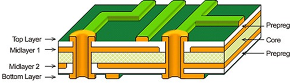
Image source: sfxpcb.com
Six Layer PCB Stackup
A six layer PCB stackup is used for PCBs with high chip density and clock frequency. It helps improve signal integrity as the signal layer and the ground layer are adjacent. Hence, it provides better control for each layer. Moreover, the additional ground layer also improves the absorption of magnetic lines, providing a return path for each signal layer.
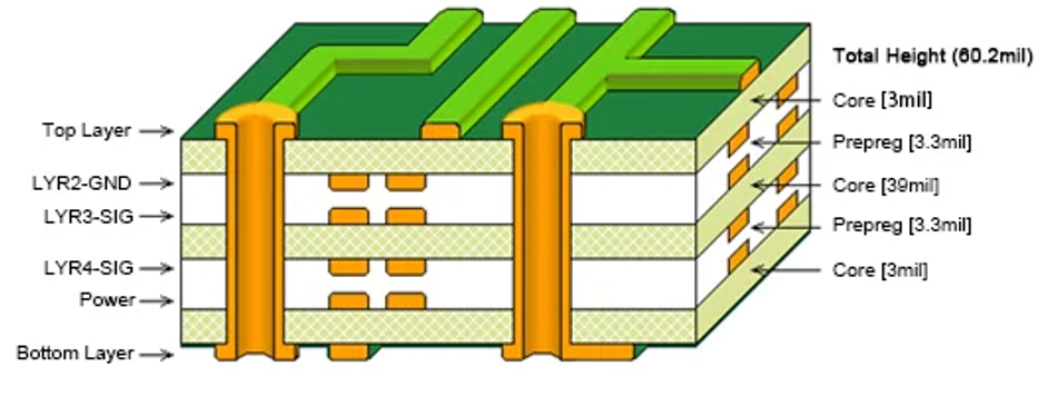
Image Source:Reversepcb
Design Considerations for PCB Stackup
An optimal PCB stackup design strategy is a combination of several critical aspects to ensure signal integrity, performance, and manufacturability. Here is a closer look at these critical factors:
Signal Integrity
Strategize the layout of signal layers to mitigate signal degradation and uphold strong signal integrity. Precise layer ordering, impedance control, and controlled dielectric constants are vital for addressing issues like crosstalk, signal reflections, and impedance mismatches.
Layer Count
Select the appropriate number of layers based on circuit complexity and required functionality, factoring in signal density, power distribution, and noise isolation.
Power and Ground Planes
Assign dedicated power and ground planes to establish a stable, low-impedance power distribution network. Ground planes aid in noise reduction, signal enhancement, and thermal dissipation.
Plane Decoupling
Integrate decoupling capacitors near power and ground plane pairs to suppress high-frequency noise and furnish clean power to sensitive components. Strategic placement and selection of decoupling capacitors are pivotal for effective decoupling.
EMI/EMC Considerations
Strategize the stackup layout to minimize electromagnetic interference (EMI) and guarantee electromagnetic compatibility (EMC). This entails meticulous positioning of signal and power planes, potential utilization of shielding layers, and adherence to proper grounding techniques.
Further Reading: EMI Shielding: Protecting Electronic Devices in a Noisy World
Thermal Considerations
Implement thermal vias and distribute thermal planes within the stackup to regulate heat dissipation, considering component-generated heat and ensuring sufficient thermal management.
Manufacturing Constraints
Account for the manufacturing capabilities and constraints of the PCB manufacturer, including minimum track width and spacing, minimum drill size, and material availability, during stackup design.
Signal Layer Ordering
Determine the sequence of signal layers in the stackup to mitigate crosstalk and streamline routing efficiency. Grouping high-speed signal layers and segregating them from low-speed layers can aid in signal integrity management.
Controlled Impedance
Design the stackup with controlled impedance for critical high-speed signals by calculating and regulating trace widths, dielectric thickness, and layer separation to achieve desired impedance values.
Material Selection
Opt for suitable laminate materials based on required electrical performance, thermal characteristics, and cost considerations. Different materials possess varying dielectric constants, loss tangent values, and thermal conductivities that can impact overall PCB performance.
Cutting-Edge Stackup Strategies
Enhancing High-Speed Signals
High-speed electronic applications demand meticulous stackup configurations to maintain signal integrity and minimize crosstalk. The key to achieving this lies in the precise control of impedance and the strategic placement of layers within the PCB stackup.
How Impedance Control Affects PCB Stackup
Impedance control ensures that the signal travels without reflection or loss of power. Hence, it’s a critical aspect of high-speed designs. It involves matching the impedance of the PCB traces with the source and load impedances. Engineers use specific stackup configurations to achieve a uniform impedance profile across the board, which is essential for preventing signal degradation over high-speed transmission lines.
Recommended Reading: Controlled Impedance: A Comprehensive Guide
Crosstalk Reduction
Crosstalk reduction is a vital consideration that can be implemented by carefully arranging signal layers and ground planes, designers can shield high-speed signals from the electromagnetic interference caused by adjacent traces. This is where the use of pre-impregnated dielectric materials (prepreg) and varying the distance between traces comes into play.
Handling Differential Signal Pairs
Advanced concepts like differential impedance calculations come into the picture when dealing with differential signal pairs, commonly used in high-speed data buses. These calculations help in designing traces that carry differential signals, ensuring that the pair has a consistent impedance to minimize crosstalk and maximize signal integrity.
Signal Integreity Simluations
Signal integrity simulations allow engineers to model and analyze the behavior of high-speed signals within the PCB stackup before physical prototypes are built. These simulations can predict issues like signal reflections, timing delays, and potential crosstalk, enabling designers to make informed decisions about trace geometry, layer stackup, and material selection.
Thermal Management Innovations
Heat management in PCB design is as critical as managing electrical signals. Innovative stackup designs play a pivotal role in thermal management, directly impacting device performance and durability.
Implementing Thermal Vias
Thermal vias are a strategic modification in stackups, creating pathways to channel heat from hotspots to cooler board areas or heat sinks. The integration of high thermal conductivity materials, like copper planes, is also essential, as they distribute heat evenly, preventing component overheating.
Including Visual Aids
Visual aids, such as thermal layout diagrams, are instrumental in illustrating these heat management strategies. They detail the placement of thermal vias and the routing of conductive planes, offering insights into the thermal behavior of the PCB.
Overcoming Stackup Design Challenges
Balancing Performance with Practicality
Navigating the delicate balance between cost and performance is a pivotal challenge in PCB design. Engineers must make strategic decisions to meet budget constraints while maintaining high performance.
Using High-Performance Materials
One effective approach is the selective use of high-performance materials. For instance, integrating high-speed materials specifically in critical signal paths, while employing more economical substrates in less crucial areas, can significantly optimize both cost and functionality. Minimizing the use of costly manufacturing processes, such as via-in-pad techniques and reducing unnecessary layer counts, also helps in cutting costs without sacrificing the board’s functionality.
Modular Designs
Modular design practices offer another cost-effective solution, allowing the reuse of tested sub-circuits across various projects. This not only cuts down on design time and costs but also leverages the reliability of previously validated components.
These targeted strategies equip designers with practical methods to effectively manage the trade-offs between cost efficiency and optimal performance in PCB design.
Documentation
As the layers of PCB stackup increase, it also increases the circuit complexity and therefore, requires rigorous check and balance for each signal trace. Hence, documentation becomes a critical aspect of the overall fabrication process.
Typically, CAD software provides tools to document the signal traces to ease the fabrication process. They ensure that all the requirements are well-met.
Conclusion
Strategic PCB stackup design is a critical factor in the modern electronics landscape, profoundly influencing the performance and reliability of electronic systems. Thoughtful stackup design is essential for achieving optimal signal integrity, power distribution, and thermal management. As electronics continue to evolve, the importance of stackup design in meeting the demands of high-speed, high-density, and multifunctional devices cannot be overstated. Engineers and designers are encouraged to pursue continuous innovation and adhere to best practices in stackup configurations to push the boundaries of what is possible in electronic design.
FAQs
What is a PCB Stackup?
A PCB stackup is the layered structure of a printed circuit board, consisting of alternating layers of conductive copper and insulating dielectric materials. This structure defines the electrical functionality and physical layout of the PCB, including the arrangement of signal, power, and ground layers that are essential for the board's operation.
How do I choose a stackup for PCB?
Choosing a stackup for a PCB involves several considerations:
Determine the number of layers needed based on the complexity of the circuit, including the number of components and the types of signals (analog, digital, high-speed).
Assess electrical requirements such as impedance control, signal integrity, and EMC (Electromagnetic Compatibility) considerations.
Consider thermal management needs, selecting materials and layer configurations that support effective heat dissipation.
Evaluate mechanical constraints, including board thickness, flexibility, and durability requirements.
Balance cost and manufacturability, selecting materials and layer counts that meet budgetary constraints while achieving the desired performance.
What are the 4 layers of PCB stack-up?
The basic 4 layers of a PCB stack-up typically include:
Top Layer: The outer copper layer where components are mounted and traces are routed.
Ground Plane: A layer dedicated to the ground connection, which helps with noise reduction and signal integrity.
Power Plane: Provides power distribution to the components on the board.
Bottom Layer: The opposite outer layer, which can also have components and traces, similar to the top layer.
4. What are the rules for PCB layer stackup?
The rules for PCB layer stackup are designed to optimize board performance and manufacturability:
Symmetry: Stackups should be symmetrical to prevent board warping during manufacturing.
Adjacent Layer Pairing: Signal layers should be adjacent to either a ground or power plane to support signal integrity.
Impedance Control: Maintain consistent impedance across signal traces by managing the dielectric thickness and material properties.
Signal Separation: Separate high-speed signal layers from each other to reduce crosstalk.
Thermal Management: Place thermal vias and select materials that support heat dissipation for high-power components.
EMC Considerations: Design stackups to minimize electromagnetic interference, following best practices for layer arrangement and spacing.
5. Is there a standard thickness for a 12-layer PCB?
While there is no standard thickness for a 12-layer PCB, the most commonly used thickness is 1.6 mm. The standard value may not suit all types of circuits such as those requiring higher mechanical strength.