Understanding Plasma Etching: Detailed Insights into Its Techniques, Uses, and Equipment Maintenance

17 May, 2023
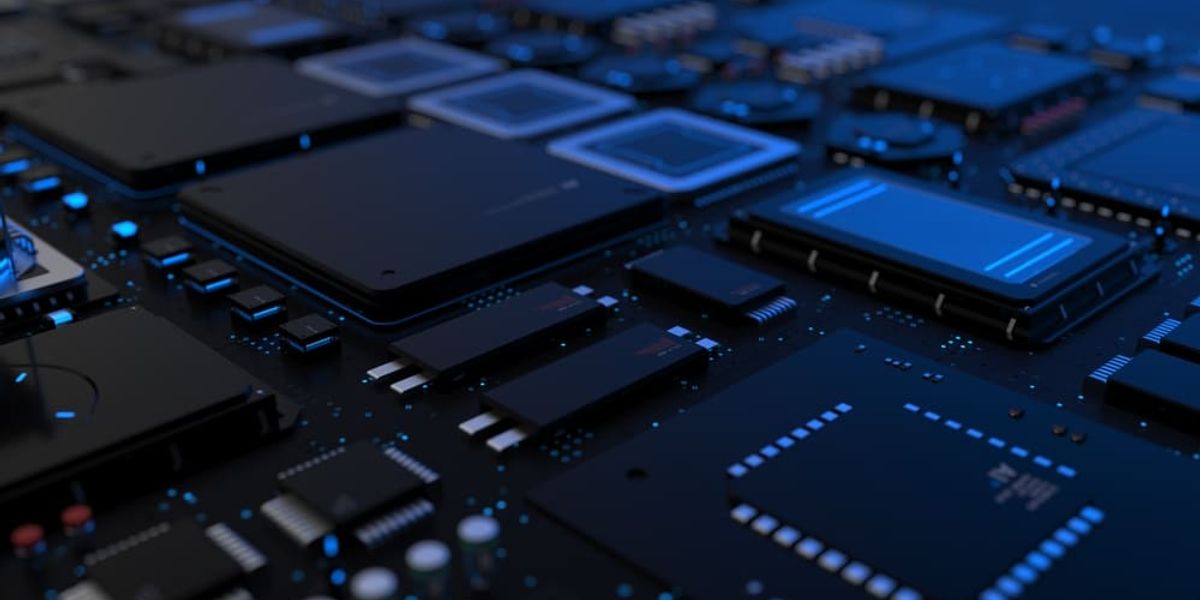
Plasma etching is a salient process in various engineering fields, especially in electronics and materials science. It's a method used to etch or carve fine patterns on the surface of substrates, such as silicon wafers used in semiconductor manufacturing. It works by creating a plasma or ionized gas within a chamber, which chemically reacts with the material on the substrate's surface, effectively removing it. Plasma etching is highly precise and allows for the creation of extremely intricate patterns at a microscopic level.
Introduction
In the thriving landscape of modern technology, the miniaturization of electronic devices has been a pivotal achievement, with plasma etching playing an unsung yet indispensable role. This process, akin to the invisible hands of a master sculptor, shapes and molds the building blocks of our digital world, from the microprocessors powering our smartphones to the memory chips in our computers.
Our quest for device miniaturization has been a ceaseless journey, one that has demanded inventive processes and techniques that can meet these challenges. One such technique is plasma etching, a process that has proven instrumental in etching nanoscale patterns onto silicon wafers, the lifeblood of the semiconductor industry.
This article delves into the intricate world of plasma etching, providing an accessible exploration of its underlying mechanisms, applications, and the pivotal role it plays in the semiconductor industry. From the basic physics that governs its operation to the advanced technologies it enables, we will unfurl the fascinating narrative of plasma etching, a story told in the language of atoms and electrons, yet integral to our everyday digital lives.
In various areas of engineering, plasma etching has proven invaluable due to its precision and flexibility. It's a cornerstone process in the manufacture of microelectronics, microelectromechanical systems (MEMS), and nanotechnology applications. The technology has evolved over the years, with advancements improving its efficiency and precision. This guide will explore plasma etching in depth, touching on its principles, types, applications, and the latest trends and developments. We'll delve into the science behind plasma etching, the equipment used, and the vital role it plays in modern technology.
1. The Fundamentals of Plasma Etching
Plasma etching, also known as dry etching, is an essential process in the fabrication of microelectronics, particularly in semiconductor manufacturing. It is the process through which patterns are carved onto substrates, mainly silicon, that form the microscopic circuits and structures in devices like computer chips and integrated circuits.
When it comes to plasma etching, plasma is the unsung hero, the invisible force that makes this innovative technique possible. Understanding the role of plasma in this process, therefore, is essential to appreciating the intricacies of plasma etching. Let's delve into the world of plasma and its fundamental importance in the context of plasma etching.
1.1. What is Plasma?
Plasma is often referred to as the fourth state of matter, distinct from solids, liquids, and gases. It is essentially a cloud of ions, electrons, and neutral particles. Unlike neutral gases, plasmas are highly reactive due to their charged particles, which are what make them so useful in processes like plasma etching. Plasma can be generated from a variety of gases, with the choice of gas heavily influencing the etching process. This is because the gas species used to form the plasma determines the type of ions available to react with the material surface during etching.
2. Role of Plasma in Plasma Etching:
In the plasma etching process, a carefully selected gas is introduced into a reaction chamber. This gas is subjected to a strong electric field, typically through the application of radio frequency (RF) power. This energy input ionizes the gas, creating a plasma. This plasma is composed of various particles, including ions and free radicals, which are both crucial to the etching process.
The role of the plasma is twofold: physical sputtering and chemical reaction. The ions in the plasma are accelerated towards the wafer due to the electric field in the chamber. When these ions collide with the wafer surface, they physically dislodge or 'sputter' material from the surface. This is the physical aspect of plasma etching.
At the same time, the free radicals in the plasma can chemically react with the material on the wafer. These reactions can produce volatile compounds that can be easily removed from the wafer surface, resulting in etching at the atomic level. This is the chemical aspect of plasma etching.
Recommended Reading: Dry Etching vs Wet Etching: Everything You Need To Know
2.1 What is the Plasma Etching Process?
At its core, plasma etching is a subtractive manufacturing process that uses plasma to selectively remove material from a substrate's surface. The process begins with the formation of plasma in a chamber, also known as a reactor. The plasma forms when a gas, often a mixture of reactive species such as fluorine or chlorine, is subjected to a strong electric field. The field excites the gas molecules, causing them to ionize and form a plasma.
Inside the reactor, the substrate to be etched is placed on a temperature-controlled platen. The substrate is typically coated with a layer of material to be etched, and a patterned layer of photoresist acts as a mask, protecting areas not to be etched. The plasma's reactive species are drawn to the substrate's surface, where they react with the unmasked material. The reaction forms a volatile byproduct, which is removed from the chamber, leaving behind the etched pattern on the substrate's surface.
The process of plasma etching is highly controllable, allowing for precise etching depths and patterns. By varying the type of gas used, the pressure in the chamber, the power applied to generate the plasma, and the temperature of the substrate, engineers can control the etching rate, selectivity, and profile. This versatility makes plasma etching a key process in various engineering fields, from semiconductor manufacturing to the fabrication of microelectromechanical systems (MEMS).
2.2 The Physics Behind Plasma Etching
Plasma etching involves a complex interplay of physical and chemical interactions. At its core, plasma etching exploits the high reactivity of plasma, a state of matter composed of ions, electrons, and neutral particles. The plasma is generated by applying an electric field to a gas, which ionizes the gas molecules. The ionized gas, or plasma, has unique properties that make it suitable for precision etching.
In the plasma state, gas molecules are excited and ionized, leading to the creation of free electrons and ions. The ions in the plasma are positively charged and are attracted towards the substrate surface, which is typically negatively biased. This bias sets up an electric field in the plasma sheath, the region adjacent to the substrate surface. The electric field accelerates the ions towards the substrate, giving them enough energy to physically dislodge atoms from the substrate surface upon impact, a process known as physical sputtering or ion bombardment.
Physical sputtering, however, is a secondary mechanism in plasma etching. The primary etching mechanism is chemical in nature. The free radicals in the plasma, which are electrically neutral but highly reactive, diffuse across the plasma sheath and reach the substrate surface. Here, they react with the material on the substrate surface, forming volatile byproducts that can easily be pumped away. This chemical reaction is selective, occurring only in areas not protected by the photoresist mask, and results in the removal of material from the substrate surface.
The balance between physical sputtering and chemical etching determines the etch profile. Ion bombardment enhances the rate of chemical etching by removing reaction byproducts and providing energy to overcome reaction barriers. However, too much ion bombardment can lead to physical damage of the substrate and a rough etch profile. On the other hand, too little ion bombardment can lead to low etch rates and the formation of a polymer layer on the substrate surface, which can inhibit etching. By carefully controlling the etching parameters, such as gas composition, chamber pressure, and power applied, it's possible to achieve an optimal balance between physical sputtering and chemical etching, resulting in high-quality etch profiles with precise control over depth and shape.
2.3 The Chemistry of Plasma Etching
Plasma etching relies heavily on the chemical reactions that take place between the plasma species and the material on the substrate surface. This process is primarily driven by reactive species in the plasma, which are typically free radicals created from the ionization of the process gas. These free radicals are highly reactive and readily participate in chemical reactions on the substrate surface.
Fluorocarbon gases, such as CF4 and CHF3, are commonly used in plasma etching due to their high reactivity and the volatility of their reaction products. When a fluorocarbon gas is ionized, it generates a variety of plasma species, including CFx (x=1-3) radicals and F atoms. These species are the primary etchants in plasma etching of silicon and silicon compounds, which are widely used in semiconductor manufacturing.
Upon reaching the substrate surface, the CFx radicals and F atoms react with the silicon atoms on the substrate surface. The reaction between F atoms and silicon results in the formation of silicon tetrafluoride (SiF4), a volatile compound that can easily be removed from the substrate surface. The reaction with CFx radicals also leads to the formation of volatile compounds, such as SiF4 and carbon monoxide (CO), which can be pumped away, leaving behind a clean, etched surface.
The chemical reactions in plasma etching are highly selective, thanks to the use of a photoresist mask. The mask protects certain areas of the substrate surface from the plasma species, preventing etching in those areas. Thus, the pattern of the photoresist mask is transferred to the substrate surface through the etching process.
The selectivity of the etching process can be further enhanced by adding an oxygen-containing gas to the process gas. The oxygen reacts with the photoresist to form a protective oxide layer, reducing the etching rate of the photoresist and improving the selectivity between the photoresist and the underlying material. This technique, known as oxygen plasma ashing, is commonly used in the fabrication of semiconductor devices to achieve high-resolution patterns with excellent selectivity.
In addition to the reactive plasma species, the ions in the plasma also play a role in the etching process. The ions are accelerated towards the substrate surface by the electric field in the plasma sheath, where they can physically sputter atoms from the substrate surface or provide energy to drive chemical reactions. However, the contribution of ions to the overall etching process is usually small compared to that of the reactive plasma species. The primary role of the ions is to enhance the etching rate and control the etch profile by influencing the directionality of the etching process.
3. Types of Plasma Etching
The etching process varies depending on the desired output and the material being processed. The two most commonly employed plasma etching techniques are Reactive Ion Etching (RIE) and Deep Reactive Ion Etching (DRIE). Both techniques use plasma to generate reactive species, but they differ significantly in their operation, application, and the results they produce.
3.1 Reactive Ion Etching (RIE)
Reactive Ion Etching (RIE) is a versatile and commonly used plasma etching technique. Its operation relies on the dual mechanisms of chemical reaction and physical sputtering. Reactive species generated from the ionization of the process gas chemically react with the substrate material, while the ions, accelerated by the electric field in the plasma sheath, physically sputter atoms from the substrate surface.
The RIE process begins with the introduction of a process gas into the etching chamber. The gas is typically a compound that contains a halogen atom, such as fluorine or chlorine, because of their high reactivity. An RF power is applied to the electrodes to generate the plasma. The reactive species produced in the plasma react with the substrate material, forming volatile reaction products that can be removed by the vacuum system.
The major advantage of RIE over other etching techniques is its anisotropy. The directionality of the ions in RIE leads to a predominantly vertical etch profile, which is crucial for creating high-resolution patterns in semiconductor fabrication. The reactive species can only reach the substrate surface from above, so the etching process is mainly confined to the vertical direction, ensuring that the etching rate in the horizontal direction is much lower than that in the vertical direction.
RIE also offers excellent selectivity between different materials. The selectivity is determined by the choice of the process gas and the etching parameters, such as the gas pressure, the RF power, and the substrate temperature. By carefully optimizing these parameters, a high etching rate for the target material and a low etching rate for the mask material can be achieved, allowing for precise pattern transfer.
However, RIE also has its limitations. The etching rate and the etch profile can be affected by various factors, including the gas chemistry, the plasma density, and the ion energy. These factors can lead to non-uniform etching and changes in the etch profile over time, which can compromise the quality of the etched patterns. Moreover, the RIE process can cause damage to the substrate material due to the high-energy ions bombarding the substrate surface, which is a major concern in semiconductor fabrication.
Recommended Reading: Reactive Ion Etching: A Comprehensive Guide
3.2 Deep Reactive Ion Etching (DRIE)
Deep Reactive Ion Etching (DRIE) is a highly specialized plasma etching technique that emerged as a solution for fabricating deep microstructures with high aspect ratios. The term 'aspect ratio' in microfabrication refers to the ratio of the depth to the width of the etched features. DRIE is well-known for its ability to etch vertical, smooth-walled structures with aspect ratios exceeding 50:1, something that conventional RIE struggles to achieve.
DRIE operates on a time-multiplexed sequence of two distinct processes: the etching phase and the passivation phase. This cycle is often referred to as the Bosch process, named after the German company Robert Bosch GmbH, which first introduced it.
In the etching phase, a highly reactive gas such as sulfur hexafluoride (SF6) is introduced into the etching chamber. RF power is applied to generate a plasma, and the fluorine ions from the SF6 plasma react with the silicon on the wafer, creating a volatile byproduct that gets evacuated by the vacuum system. The high-energy ions sputter the substrate, resulting in a highly anisotropic etch.
The passivation phase follows the etching phase. In this phase, an inert gas like octafluorocyclobutane (C4F8) is used. When ionized, C4F8 forms a Teflon-like polymer on all exposed surfaces. This polymer layer is highly resistant to the reactive ions, effectively protecting the sidewalls from further etching in the next cycle.
These two phases are alternated repeatedly, with each cycle lasting a few seconds. The repeated sequence of etching and passivation results in a highly anisotropic, deep, and straight etch profile, enabling the creation of deep trenches and high aspect ratio structures.
DRIE's capability to create high aspect ratio structures has opened up new possibilities in MEMS fabrication, particularly in the manufacturing of accelerometers, gyroscopes, and microfluidic devices. However, the process does present some challenges. The primary one is the 'scalloping' effect, which is the result of the cyclical nature of the process. Scalloping refers to the slightly wavy sidewall profile that can occur due to the alternating etching and passivation cycles.
4. Plasma Etching Equipment and Its Maintenance:
The task of plasma etching is performed using specialized equipment designed to precisely control the many variables involved. Ensuring the reliability and longevity of this equipment calls for regular maintenance, a fundamental aspect of effective operation in the semiconductor industry.
4.1 Types of Plasma Etching Equipment
The types of plasma etching equipment mainly depend on the etching technique and the specific requirements of the fabrication process. The common types of plasma etching equipment are parallel plate etchers, reactive ion etchers, and inductively coupled plasma etchers.
Parallel Plate Etchers:
Parallel plate etchers, also known as planar or diode etchers, are the simplest form of plasma etching systems. In these systems, the wafer is placed on the grounded electrode, and the RF power is applied to the other electrode. The plasma is formed between the two parallel plates, and the etching process takes place. The simplicity and cost-effectiveness of parallel plate etchers make them a suitable choice for less demanding applications.
Reactive Ion Etching:
Reactive Ion Etching (RIE) systems are a step up from parallel plate etchers. In RIE systems, the lower electrode, where the wafer is placed, is RF powered while the upper electrode is grounded. This setup creates a DC bias on the wafer, attracting positive ions from the plasma towards the wafer surface, thus enhancing the etching rate and providing a more anisotropic etch. RIE systems are widely used for more demanding applications requiring high precision and control.
Inductively Coupled Plasma:
Inductively Coupled Plasma (ICP) etching systems are the most advanced type of plasma etching equipment. In ICP systems, the plasma is generated by an RF coil, usually located above the etching chamber. This arrangement allows for high plasma densities and lower operating pressures, resulting in higher etching rates and better control over the etching process. ICP systems are commonly used in high-volume production environments and applications that require the utmost precision, such as advanced semiconductor fabrication.
While each type of etching equipment has its strengths, the choice of equipment depends on several factors, including the desired etch rate, the required etch profile, the type of material to be etched, and the overall requirements of the fabrication process. A thorough understanding of the principles of plasma etching and the specific requirements of the application are critical in choosing the right etching equipment.
4.2 Maintaining Plasma Etching Equipment
The maintenance of plasma etching equipment is a complex task, requiring both preventive and corrective actions to ensure optimum performance and longevity. Understanding the operational aspects of the equipment, including the etching process itself, the mechanical and electrical components, and the safety systems, is crucial for effective maintenance.
Preventive maintenance of plasma etching equipment typically involves regular inspections and servicing to prevent potential failures. This includes checking the integrity of the plasma chamber, as plasma can cause significant wear and tear on the chamber walls over time. Regular cleaning of the chamber is also necessary to prevent the build-up of etched material, which could negatively impact the etching process.
Another key component in preventive maintenance is the regular inspection and replacement of consumables, such as etching gases and electrodes. The etching gases should be checked for purity and pressure, as any deviations can lead to inconsistent etching results. Electrodes, on the other hand, undergo erosion during the etching process and need to be replaced at regular intervals to maintain the efficiency of the etching process.
For the electrical components, regular checks for insulation failures and signs of overheating are essential. Additionally, the RF generator, which is critical for plasma generation, requires regular tuning and calibration to ensure it is delivering the correct power levels.
Corrective maintenance, on the other hand, involves addressing any issues or failures that arise during operation. This could include repairing or replacing failed components, troubleshooting process inconsistencies, or resolving safety system alerts. Timely corrective actions can prevent minor issues from escalating into major problems that could cause significant downtime or damage to the equipment.
Ultimately, maintaining plasma etching equipment requires a holistic approach that takes into account the intricate interplay between various components and systems. Regular training for maintenance personnel, adherence to maintenance schedules, and prompt resolution of any identified issues are crucial to keeping the etching equipment in top condition and ensuring high-quality etching results.
5. Applications of Plasma Etching
Plasma etching, with its precise, anisotropic, and selective etching capabilities, has found wide-ranging applications in various industries. While most commonly associated with the semiconductor industry, its influence extends far beyond, impacting fields such as material science, optics, and even biotechnology. Let's explore some of these applications in more detail.
5.1 Plasma Etching in Microfabrication
Plasma etching plays an indispensable role in the field of microfabrication, where it is utilized to shape and pattern the tiny structures that constitute integrated circuits (ICs) and microelectromechanical systems (MEMS). Microfabrication demands extreme precision and control over the process parameters to ensure the integrity of the miniature features being created, and plasma etching meets these requirements proficiently.
Integrated circuits, the heart of every electronic device, are fabricated using multiple layers of different materials, each of which needs to be precisely patterned to form the necessary circuit elements. Plasma etching, with its capability to provide anisotropic etching, is heavily used in this process. For instance, the fabrication of CMOS (Complementary Metal-Oxide-Semiconductor) devices, a key component in modern digital circuits, requires etching steps to define the gate, source, and drain regions of the transistor. In a typical CMOS process flow, the gate is defined by etching polysilicon using a chlorine-based plasma, while the source and drain regions are etched into the silicon substrate using a fluorine-based plasma.
In MEMS technology, plasma etching is used to create the micro-sized mechanical elements like gears, levers, and cantilevers. A key application is in the fabrication of microscale accelerometers and gyroscopes for inertial sensing, which are found in devices ranging from smartphones to aerospace navigation systems. Deep reactive-ion etching (DRIE) is particularly useful for these applications due to its capability to create high-aspect-ratio structures, such as the long, narrow trenches required in comb-drive actuators.
Beyond ICs and MEMS, plasma etching also finds use in the fabrication of other micro and nano-scale devices, such as photonic crystals, microfluidic devices, and nanowire-based sensors. The capability of plasma etching to work with a wide range of materials, combined with its precision and control, makes it a critical tool in the microfabrication toolkit.
5.2 Plasma Etching in Semiconductor Manufacturing
The manufacturing process of semiconductors is intricately tied to the use of plasma etching. The process starts with a silicon wafer, onto which various layers of materials are deposited and then patterned using photolithography. The exposed areas are then etched away using a plasma, revealing a carefully crafted design that forms the basis of transistors, diodes, and other fundamental components of electronic devices.
Plasma etching is particularly critical in the creation of FinFETs, a type of transistor that is widely used in modern processors due to its excellent performance characteristics. In a FinFET, the channel of the transistor is shaped into a thin vertical fin, which allows for better control of the current flow and reduces leakage. The creation of these fins involves etching away the silicon around them, a process that requires the high aspect ratio etching capabilities of DRIE.
Besides FinFETs, plasma etching is also used in the manufacturing of DRAM (Dynamic Random-Access Memory) cells. The capacitor in a DRAM cell, which stores the bit of data, is typically located in a trench etched into the silicon substrate. The creation of these trenches requires precise control over the etching depth, which is provided by the time-controlled nature of plasma etching.
In semiconductor manufacturing, plasma etching also facilitates the formation of vias and trenches in the process of interconnect fabrication. This is the stage where the different transistors on a chip are wired together to form a complete circuit. The vias, which are small holes, are used to connect different layers of wiring, while the trenches are where the actual wires are laid. Both of these structures are created by etching away the dielectric layer, usually silicon dioxide, using a fluorocarbon-based plasma.
The precision and versatility of plasma etching, its ability to work with a wide range of materials, and its compatibility with photolithography make it an essential technique in semiconductor manufacturing. Without it, the miniaturization trend that has driven the semiconductor industry for decades would not have been possible.
5.3. Optoelectronics and Photonics:
Plasma etching has found significant application in the fields of optoelectronics and photonics, enabling the creation and refinement of devices that intersect the realms of light and electronics. In the fabrication of light-emitting diodes (LEDs), for instance, plasma etching is employed to precisely structure the semiconductor layers, which is particularly vital in the production of micro-LEDs and nano-LEDs. This precise structuring facilitates better control over the light-emission properties of the LEDs.
In the realm of semiconductor lasers, such as those utilized in fiber-optic communication systems or compact disc players, plasma etching is employed to define the size and shape of the active region where light amplification takes place. The precision of plasma etching is key in determining specific properties of the laser, such as its wavelength and power output.
The production of photovoltaic cells, or solar cells, also benefits from the use of plasma etching. The process is used to texture the surface of the silicon wafer, creating a landscape of microscopic pyramids. This texturing process enhances the overall efficiency of the cell by reducing reflection and increasing the path length of light within the cell, thus improving its light-trapping ability.
Photonic crystals, which are materials characterized by a periodic variation in refractive index, are another application area for plasma etching. These crystals can manipulate photons in a way analogous to how semiconductors manipulate electrons, leading to the creation of "band gaps" that can control the flow of light. Plasma etching is used to fabricate these intricate structures, allowing for the creation of devices that can control and manipulate light in novel ways.
From enabling the efficient conversion of sunlight into electricity to creating precise and compact light sources, plasma etching has been instrumental in the advancement of optoelectronics and photonics. Its ability to create precise and complex structures on a microscopic scale makes it an invaluable tool in these rapidly evolving fields.
6. Conclusion
The role of plasma etching in numerous technological fields cannot be overstated. It has been instrumental in the fabrication of semiconductors, where it's used for shaping transistors, creating DRAM cells, and making interconnects. The distinct advantages offered by plasma etching, such as the ability to etch high aspect ratio structures and to control the etching rate precisely, have made it the method of choice in microfabrication.
The technological progress in the semiconductor industry, following Moore's law, has been largely enabled by advances in plasma etching. As devices continue to shrink, and new materials are introduced, new challenges arise that require the development of new etching techniques and recipes. The field of plasma etching, therefore, is one that will continue to evolve and innovate in response to the needs of the semiconductor industry.
The equipment used for plasma etching is complex and needs careful maintenance to ensure optimal performance. The choice of equipment depends on the specific requirements of the process, such as the type of etching (RIE or DRIE), the material to be etched, and the desired etching characteristics. Proper maintenance of the equipment involves regular inspections, cleaning, and replacement of worn-out components.
7. FAQs
Q: What types of materials can be etched using plasma etching?
A: A wide range of materials can be etched using plasma etching. This includes but is not limited to silicon, silicon dioxide, silicon nitride, and various metals. The specific gas mixture used in the plasma determines which materials can be etched.
Q: What's the difference between RIE and DRIE?
A: RIE, or Reactive Ion Etching, is a type of plasma etching where the material is removed by chemical reactions between the ions in the plasma and the material surface. DRIE, or Deep Reactive Ion Etching, is a variant of RIE that's designed to create deep, high-aspect-ratio structures. It alternates between etching and passivation steps to achieve this.
Q: How is plasma etching used in the manufacturing of semiconductors?
A: In semiconductor manufacturing, plasma etching is used to create various structures on a silicon wafer, such as transistors, capacitors in DRAM cells, and interconnects. It's also used to create vias and trenches for the wiring of the different components on the chip. The process involves depositing a layer of material on the wafer, patterning it using photolithography, and then etching the exposed areas with a plasma.
Q: Why is plasma etching preferred over other etching methods?
A: Plasma etching offers several advantages over other etching methods. It allows for anisotropic etching, which means it can etch in one direction more than others, allowing for the creation of high-aspect-ratio structures. It also provides precise control over the etching rate, which is critical for ensuring the accuracy of the etched structures. Finally, it's compatible with a wide range of materials and is well suited for integration with other semiconductor fabrication processes.
Q: What maintenance is required for plasma etching equipment?
A: Plasma etching equipment requires regular maintenance to ensure optimal performance. This includes cleaning the chamber to remove any buildup of etching byproducts, replacing worn-out components such as the electrodes and seals, and inspecting the equipment for any signs of damage or wear. The specific maintenance procedures and schedules depend on the type of equipment and the etching processes that it's used for.
References:
https://www.sciencedirect.com/topics/materials-science/plasma-etching
https://www.plasmaetch.com/plasma-etching.php
https://plasmatreatment.co.uk/pt/plasma-treatments/plasma-etching