Design for Manufacture Considerations for Ball Grid Array (BGA) Packages
Last updated on 04 May, 2024
The miniaturization of electronics is widely attributed to advances in semiconductor technology as observed by Moore’s Law, but many overlook the design and manufacturing challenges involved in utilizing small device packages such as ball grid arrays.
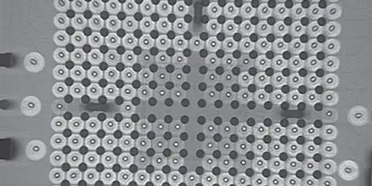
BGAs (Ball Grid Array) are a type of lead-less surface mount semiconductor package that, as the name suggests, features an array of spherical solder balls on the underside of the package.
Many motherboard control chips utilize this packaging technology. Memory chips utilizing this package technology can double or triple their capacity without increasing in size and compared to other packages, BGA offer higher pin counts, superior heat dissipation and enhanced electrical performance in a smaller volume.
The technological success of compact packages including BGA packages allow us to have supercomputers that fit in the palm of our hands. Microprocessors, FPGAs, and memory chips are increasingly being offered in BGA type packages as general PCB assembly capabilities catch-up and the demand for small and powerful electronics continues to increase. However, their utilization poses challenges for PCB layout and manufacture.
Small-pitch BGA packages and packages with higher pin counts encroach on the limits of many modern assembly houses’ capabilities and call for complex PCB stack-ups and via technologies, not to mention the power and heat dissipation and signal integrity of the overall design must be considered.
Designing with BGAs require significant investment and preparation in terms of researching manufacturing and design techniques, and money as the techniques required to fully route-out fine-pitch and larger BGA packages are advanced and costly, and poor design decisions could increase the manufacturing costs by several factors.
Before choosing to design with BGA packages, designers should acquaint themselves with the capabilities of their PCB manufacturer and assembly house and familiarize themselves with the design techniques needed to achieve a reliable design at the best price possible. Failure to do so could result in unexpected expenses or wasted time reworking or restarting a design.
In this article, we summarize a few BGA design considerations designers should be aware of before beginning a BGA design, especially fine-pitch BGAs (0.5mm pitch and below BGAs).
Routing Traces Between BGA Pads
The number of traces that can be routed between BGA pads is determined by the BGA pitch (center-to-center spacing) and the PCB fabricators capabilities. Typically traces can be routed between pads for 0.5mm and above pitch BGAs. Two can be squeezed in between 0.8mm pitch and above pitch BGAs. For 0.4mm pitch and below BGAs, routing between them is not feasible due to trace width and spacing limitations. Many PCB manufacturers can produce 4mil (0.1mm) traces reliably and 3-3.5mil is not uncommon if used for limited to necking. Necking of traces is where the trace thickness is reduced in select areas. Necking can allow for routing between 0.5mm pitch BGAs pads and routing of more than one trace between pads of larger pitch BGAs.
BGA Pad Size
To route traces, BGA pads should be sized accordingly to ensure adequate spacing between pads. Manufacturers will modify production files to fit their processes and if the spacings are not adequate, excess copper may be shaved off. If the BGA pads are cut into irregular shapes, the quality of the solder joints could be affected.
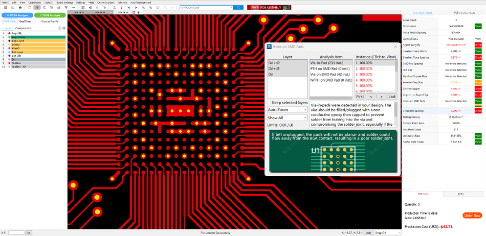
Via-in-Pad via filling and capping
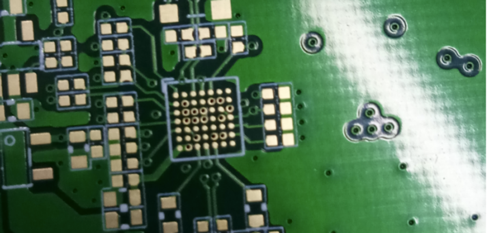
When pad spacing is tight and routing between pads is not possible (such as for 0.4mm pitch BGAs), vias can be placed directly on top of BGA pads (via-on-pad), allowing for signal transfer to the inner or bottom layers. However, it is important that these vias are filled and capped. If not, solder joint defects are almost certain to occur due to the non-planar surface and solder leaking through the vias.
The via filling and capping process involves using specialized equipment to fill the vias with a non-conductive epoxy then capping them by plating over the via, essentially adding a pad on top of the via. The plated over vias are visually indistinguishable from regular BGA pads to the naked eye.
Tenting of Regular BGA Vias
Regular vias between BGA pads should be covered to prevent the solder ball and molten solder paste wicking away from the BGA pads, short circuits and to protect the via from environmental contaminants. Various methods are available for different quality levels.
The most basic is to simply cover the vias with solder mask i.e. tent the vias. The solder mask offers a fine layer of protection from contaminants and electrical shorts, however, the level of coverage depends on the viscosity of the solder mask oil and via size. The holes of larger vias may not be fully covered and there is the risk of the via popping during reflow if there is moisture inside the via.
Solder mask plugging is another option which adds an extra production step to press solder mask oil into the vias before the general solder mask covering. This ensures that the via barrel is blocked with solder mask but is not guaranteed to be fully filled.
The optimal solution is to have all vias filled with epoxy but since this an expensive process, this is usually reserved for high demand applications where via reliability and lifetime is important.

Via-In-Pad and HDI Design
For fine-pitch BGA chips where traces cannot be routed between pads, it is advisable to utilize a HDI (high-density-interconnect) design with blind and buried vias. For example, mobile phone boards typically have small BGA chips that do not allow for routing between pads.
A HDI design with blind and buried vias can be used to make maximum use of the available space in all layers however, the specific stack-up, types of blind/buried vias and total number of layers can have a significant impact on the PCB manufacture cost. It is recommended to consider all possible options on a cost-benefit basis before beginning a design and choosing the types of blind buried vias to use.
Tools for Improving BGA PCB Design
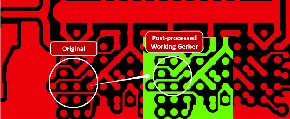
Many considerations go into designing a PCB based on a BGA device beyond the scope of this article. HQDFM is a free software developed by HQ NextPCB (HQ Electronics) that inspects Gerber files or OBD++ files for common design for manufacture errors that may affect reliability, cost or manufacturability.
Via-In-Pad Design
HQDFM can detect via-in-pads and reminds designers that via-in-pads should be filled and plated to prevent solder defects and that this increases production costs significantly. If these can be moved away from the pad and converted to regular vias, this will remove the need for via filling and capping.
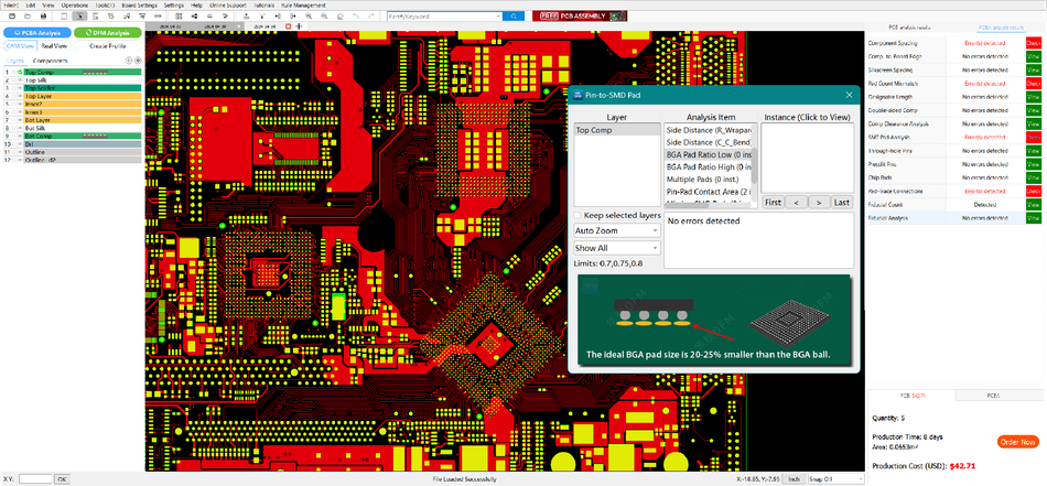
Pad-to-Pin Size Ratio
HQDFM can compare the solder pad size to the size of the BGA ball. A pad diameter less than 20% smaller than the BGA pin size could lead to insufficient space for routing, while more than 25% might result in poor solder joints. In such cases, design engineers need to adjust the ratio of pad diameter to BGA pin diameter.
HQDFM can also detect areas where trace widths and spacings are inadequate, opened vias, poor component placement and spacing and more not just related to BGA design.
HQDFM is a free PCB design analysis software covering bare board and populated PCB analysis. With over 200 inspection items under 30 DFM and DFA categories including trace, solder mask and drill clearances, pads dimensions, shorts/opens, drill hole sizes and solder mask dams. HQDFM also provides tools for the designing and manufacturing PCBs including an impedance calculator, panelization tool, footprint, BOM and centroid file checker.
Transform your workflow and swiftly integrate DFM methodologies into your product development with the HQDFM desktop suite from HQ Electronics (NextPCB).