CCD vs CMOS Image Sensors: A Comprehensive Guide for Engineering Professionals
CMOS and CCD sensors both convert light into electronic signals, with CMOS using pixel-level transistors for faster, energy-efficient processing, while CCD transfers charge across the chip for superior image quality but with slower speed and higher power consumption.

21 Aug, 2024. 27 min read
Introduction
CCD (Charge-Coupled Device) and CMOS (Complementary Metal-Oxide-Semiconductor) sensors are crucial in modern imaging, impacting fields from industrial automation to medical diagnostics. These sensors convert light into electrical signals, which is essential for digital imaging. CCD sensors, known for superior image quality and low noise, excel in applications like astronomical observations and high-end medical imaging. CMOS sensors, with lower power consumption and faster processing, are ideal for smartphones and automotive cameras.
Recent innovations have enhanced both technologies. Backside illumination in CMOS sensors boosts light sensitivity, while advancements in CCD technology improve charge transfer efficiency and reduce noise. These developments expand the possibilities for engineering applications. High-speed CMOS sensors in industrial automation enable rapid inspection, and advanced CCD sensors in medical imaging provide the resolution necessary for detailed diagnostics. Staying updated on these technologies allows engineers to drive innovation and achieve superior results.
History of CCD and CMOS Imaging Sensors
Digital imaging technology has seen profound transformations, significantly influenced by the arrival of the CCD in the late 1960s and the later adaptation of CMOS technology for imaging sensors in the early 1990s.
Recommended reading: IC Package Types: A Comprehensive Guide
Before the development of CCD and CMOS imaging sensors, imaging technology relied on more rudimentary forms such as vacuum tube technology, including the Vidicon and its variants used in television cameras and early video equipment. These devices converted optical images into electronic signals using a light-sensitive surface and an electron beam that scanned the surface to create a video signal. Although effective for their time, these technologies suffered from various limitations, such as lower image quality, higher susceptibility to image burn-in, and greater sensitivity to light conditions, often resulting in significant image degradation over time. The development of solid-state devices like CCD and CMOS sensors represented a step forward, offering more reliability, improved image quality, and lower power consumption.
The Development of CCD Technology
Invented in 1969 by Willard Boyle and George E. Smith at AT&T Bell Labs, CCD technology was initially explored for computer memory but soon proved invaluable for digital imaging.[1] The introduction of the first commercial CCD video camera by Fairchild Semiconductor in 1975 marked a pivotal moment, setting new standards for image clarity and sensitivity in applications ranging from astronomy to medical imaging.
The Rise of CMOS Imaging Sensors
While CMOS technology had been utilized in electronics for several decades, its application in imaging sensors was pioneered by Eric Fossum and his team at NASA’s Jet Propulsion Laboratory in the early 1990s.[2] This innovation integrated transistor functions at each pixel site, significantly improving the efficiency and speed of image processing. The development of CMOS imaging sensors revolutionized consumer electronics, particularly within the burgeoning mobile phone market, due to their lower power consumption and cost-effective production.
These innovations have opened the door to the diverse applications of modern digital imaging, demonstrating significant advancements in capturing and processing visual information with increasing accuracy and detail.
Understanding CCD and CMOS Sensors
How do CCD Sensors work?
CCD sensors revolutionized imaging technology by providing a way to convert light into electronic signals with high precision. These sensors consist of an array of capacitive bins that collect and transfer electric charge through a process known as charge transfer. When photons hit the CCD sensor, they generate electron-hole pairs in the silicon substrate, which are then stored in potential wells created by electrodes, forming pixels.
The working principle of CCD sensors involves the sequential transfer of charge from one pixel to the next, a process meticulously controlled by clock signals. This precise charge transfer moves the accumulated charge across the sensor to an output node, where it is converted into a voltage and then digitized. For example, in astronomical telescopes, this technology allows for the capture of faint celestial objects with remarkable clarity, as the low noise levels and high charge transfer efficiency ensure minimal signal loss.
Key advantages of CCD sensors include their low noise levels and high image quality. These attributes are crucial in applications such as medical imaging, where detailed and accurate visuals are essential for diagnostics. In scientific research, CCD sensors enable high-resolution imaging that is vital for experiments requiring exacting precision. Additionally, in high-end photography, the superior image quality provided by CCD sensors ensures that every detail is captured, making them the preferred choice for professional photographers who demand the highest fidelity in their images.
How a CCD Camera Works: Step-by-Step
A CCD camera captures and processes images through a series of steps that involve converting light into electrical signals and then into digital data. Below is a step-by-step explanation of how a CCD camera works:
1. Light Capture
The process begins when light from the scene enters the camera lens and is focused onto the CCD sensor. The CCD sensor is made up of a grid of tiny, light-sensitive elements called pixels. Each pixel is designed to capture the light that falls onto it, with the intensity of the light determining the amount of electrical charge generated within that pixel.
2. Photon to Electron Conversion
When photons (particles of light) strike the CCD sensor, they are absorbed by the silicon material in each pixel. This absorption causes the generation of electron-hole pairs within the silicon. Essentially, each photon generates an electron, and the number of electrons produced is directly proportional to the intensity of the light striking the pixel. This accumulation of electrons represents the brightness information for that particular part of the image.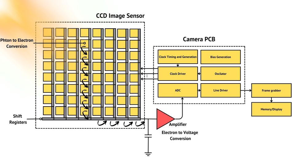
3. Charge Accumulation
Each pixel on the CCD sensor acts as a small storage well for the generated electrons. Over the duration of the exposure, the amount of charge (or number of electrons) in each pixel builds up, corresponding to the amount of light hitting that pixel. Brighter areas of the scene generate more charge, while darker areas generate less.
4. Charge Transfer
Once the exposure is complete, the camera needs to read out the image. This is where the "charge-coupled" nature of the CCD sensor comes into play. The accumulated charge in each pixel is transferred sequentially across the sensor to the readout register. This process occurs in a manner similar to a bucket brigade, where the charge from one pixel is passed to the next, eventually reaching the output node at the edge of the sensor.
Global Shutter: CCD sensors typically use a global shutter mechanism, where all pixels capture light simultaneously, preventing distortions that can occur with moving objects, unlike the rolling shutter found in some CMOS sensors.
5. Conversion to Voltage
At the output node, the charge from each pixel is converted into a voltage signal. This conversion is crucial because the resulting voltage directly corresponds to the amount of light captured by the pixel. The more charge there was in a pixel, the higher the voltage produced at the output node.
6. Analog-to-Digital Conversion
After the charge has been converted into a voltage, the next step is to convert this analog signal into digital data. This is done by an Analog-to-Digital Converter (ADC). The ADC takes the continuous voltage signals from the sensor and converts them into discrete digital values that can be processed by the camera’s electronics. The quality and resolution of the digital image are heavily dependent on the efficiency and precision of the ADC. A high-quality ADC ensures that the fine details of the captured image are preserved and accurately represented in the final digital output.
7. Image Processing
Once the image is in digital form, the camera's onboard processor performs various image processing tasks. This might include adjusting brightness and contrast, correcting color balance, reducing noise, and applying filters. Additionally, the camera might compress the image, depending on the selected file format (such as JPEG or RAW). During this stage, the camera may also apply the chosen ISO setting, which adjusts the image brightness by amplifying the digital signal. However, higher ISO settings can introduce noise, especially in low-light conditions.
How a CMOS Sensor Works: Step-by-Step
CMOS sensors are integral to modern digital imaging, particularly in devices like smartphones, digital cameras, and high-speed industrial systems. Unlike CCD sensors, CMOS sensors process image data in a way that allows for faster operation and lower power consumption. Here’s a step-by-step explanation of how a CMOS sensor works:
1. Light Capture
Just like in a CCD sensor, the process starts when light enters the camera lens and is focused onto the CMOS sensor. The CMOS sensor is made up of millions of pixels arranged in a grid. Each pixel acts as a light detector, capturing photons and converting them into an electrical charge.
2. Photon to Electron Conversion
When photons hit the CMOS sensor, they are absorbed by the photodiodes within each pixel. This absorption generates electron-hole pairs in the silicon substrate, where each photon generates one electron. The number of electrons generated in each pixel is proportional to the intensity of the light striking that pixel. Brighter areas in the image produce more electrons, corresponding to higher brightness levels.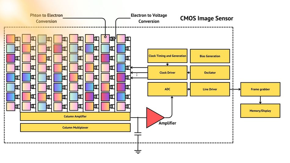
3. Charge to Voltage Conversion (at Pixel Level)
Unlike CCD sensors, where the charge is transferred across the sensor to a single readout node, CMOS sensors convert the charge to a voltage directly at each pixel. Each pixel in a CMOS sensor contains not only a photodiode but also a small amplifier, as well as other circuitry, that converts the accumulated charge into a voltage signal right within the pixel itself. This process occurs in parallel across all pixels.
Active Pixel Sensor (APS) Architecture: This architecture, known as APS, allows each pixel to operate independently, enabling faster readout speeds and more efficient processing compared to the sequential transfer in CCDs.
4. Signal Amplification and Processing
After the charge is converted to voltage at the pixel level, the signal is amplified to make it strong enough for further processing. This amplification occurs within the same pixel, minimizing the distance the signal has to travel, which reduces noise and improves image quality. In many CMOS sensors, the analog voltage signals are converted to digital signals at the column or even the pixel level by an integrated ADC. This localized conversion is one of the reasons CMOS sensors can achieve high-speed readouts.
5. Rolling Shutter Effect (if applicable)
One characteristic of many CMOS sensors is the rolling shutter effect. Because each row or column of pixels is read out sequentially rather than all at once, moving objects can appear distorted. For example, a fast-moving car might look skewed because different parts of the image are captured at slightly different times. However, advanced CMOS sensors can mitigate this effect, and some even employ a global shutter to capture all pixels simultaneously, similar to CCD sensors.
6. Digital Signal Processing
Once the signals have been converted from analog to digital, they undergo processing to produce the final image. This processing includes several steps:
Noise Reduction: Digital noise, especially in low-light conditions, is reduced through algorithms designed to clean up the image.
ISO Adjustment: The camera applies the selected ISO setting to adjust the image’s brightness. Higher ISO values amplify the signal, which can introduce noise, though CMOS sensors have made significant strides in maintaining image quality at higher ISO settings.
Color Interpolation: Since each pixel typically only captures one color (red, green, or blue), the camera must interpolate the full-color image by combining data from adjacent pixels.
Dynamic Range Adjustment: The dynamic range, or the difference between the darkest and brightest parts of the image, is adjusted to ensure that details in both highlights and shadows are preserved.
7. Image Output
After processing, the digital image is stored in the camera's memory or displayed on the device’s screen. The processed data can be saved in various formats, such as JPEG or RAW, depending on the device’s capabilities and user settings.
8. Integration and Additional Features
CMOS sensors are known for their high level of on-chip integration. In addition to the photodiode and amplifier, CMOS sensors often include circuitry for ADCs, timing control, and other processing functions directly on the sensor chip. This high level of integration not only reduces the size and cost of the camera system but also improves its overall efficiency and performance. The integrated electronics allow for real-time adjustments to ISO settings, giving users more control over image exposure, particularly in varying light conditions.
Recommended reading: Chips and Wafers: What's the Difference?
How do CMOS Sensors work?
CMOS sensors are powerful alternatives to CCD sensors, and have revolutionized the field of digital imaging. These sensors are known for their ability to integrate complex circuitry directly onto the sensor chip, allowing each pixel to contain its own amplifier and processing components. This architecture not only enhances readout speed but also reduces power consumption, making CMOS chips highly efficient.
The working principles of CMOS sensors involve several critical components. Each pixel includes a photodetector and an active transistor switch. When photons strike the photodetector, electron-hole pairs are generated, and the resulting charge is converted into a voltage signal by the transistor. This signal is then processed and read out by adjacent on-chip circuitry, which performs functions such as noise reduction and analog-to-digital conversion. Unlike CCD sensors, where charge is transferred across the chip to a common output, CMOS sensors process pixel data in parallel, significantly increasing speed.
Key advantages of CMOS sensors include their low power consumption and high operational speed. These features are particularly valuable in applications where energy efficiency and rapid data processing are crucial. For example, in mobile devices like smartphones, CMOS sensors enable high-resolution imaging while conserving battery life. Similarly, in automotive applications, the quick processing capabilities of CMOS sensors are vital for ADAS that rely on real-time visual data to enhance vehicle safety.
In the industrial automation sector, CMOS sensors excel in machine vision tasks, where their fast processing times and integration flexibility improve efficiency and accuracy. The ability to incorporate advanced processing capabilities directly onto the sensor chip simplifies system design and reduces costs, making CMOS sensors a versatile and attractive option for a wide range of engineering applications. Through their innovative design and practical advantages, CMOS sensors continue to push the boundaries of what's possible in digital imaging technology.
CCD vs CMOS: Breaking Down the Differences
Aspect | CCD Sensors | CMOS Sensors |
Structure | Uses a single readout amplifier | Each pixel has its own amplifier |
Image Quality | Typically higher image quality, especially in low-light conditions | Slightly lower image quality but improving with advancements like BSI |
Dynamic Range | Typically, a higher dynamic range | Slightly lower dynamic range |
Noise | Lower noise, especially in long exposure applications due to serial charge transfer | Higher noise due to parallel processing, but newer designs are closing the gap |
Power Efficiency | Higher power consumption | Lower power consumption |
Speed | Slower readout speeds, due to sequential charge transfer | Faster readout speeds due to parallel processing |
Integration | Limited on-chip integration, external components are often needed | High level of on-chip integration, more features on the sensor |
Cost | Generally more expensive to produce | Typically cheaper to manufacture |
The structural differences between CCD and CMOS sensors fundamentally affect their functionality and performance. CCD sensors use a single readout amplifier for the entire array, which ensures low noise levels and high image quality. However, this serial charge transfer process is slower and consumes more power. In contrast, CMOS sensors have amplifiers at each pixel, enabling parallel processing and faster readout speeds. This design, while efficient, tends to introduce more noise.
From a practical engineering perspective, these differences have significant implications. CCD sensors, with their superior dynamic range and low noise, are ideal for applications where image quality is paramount, such as in scientific imaging and high-end photography. Their downside is the higher power consumption and slower speeds, which can be limiting in time-sensitive applications.
CMOS sensors, on the other hand, are favored for their lower power consumption and high-speed capabilities, making them suitable for mobile devices and automotive applications where quick processing and efficiency are critical. The higher level of on-chip integration in CMOS sensors simplifies system design and reduces costs, despite the trade-off in noise performance and dynamic range.
Key Points:
CCD sensors offer high image quality and less noise but are slower and consume more power.
CMOS sensors provide faster readout speeds and lower power consumption but typically have higher noise levels.
The choice between CCD and CMOS sensors depends on the specific requirements of the application, balancing factors like image quality, speed, power efficiency, and cost.
Cutting-Edge Advancements in Sensor Technology
Innovations Powering the Next Generation of CCD Sensors
CCD sensors have undergone significant transformations over the decades. Recent advancements have further enhanced their capabilities, making them indispensable in high-precision imaging applications.
Improved charge transfer efficiency: A major breakthrough has been the improvement in charge transfer efficiency. This enhancement allows a higher percentage of the generated charge to reach the output node with minimal loss, which is crucial for maintaining high image quality, particularly in low-light conditions.
Improved fabrication techniques: New fabrication techniques, such as advanced lithography and etching processes, have enabled the creation of smaller, more densely packed pixels. This increase in pixel density elevates the resolution of CCD sensors, allowing them to capture finer details. These techniques also contribute to reducing the overall sensor size, broadening their applicability across various fields.
Improved Doping Processes: In terms of sensitivity and noise reduction, improved doping processes have played a pivotal role. By precisely controlling the introduction of impurities in the silicon substrate, manufacturers can significantly enhance the sensor's charge generation and transfer capabilities. This results in higher sensitivity, enabling the detection of weaker signals and producing clearer images. Furthermore, advanced pixel architectures, including multi-phase charge-coupling techniques, have been designed to minimize noise, reducing dark current and other noise sources for cleaner, more accurate images.
These innovations collectively enhance the performance of CCD sensors, making them ideal for applications requiring high sensitivity, resolution, and low noise. For instance, in scientific research, CCD sensors provide the precision needed for detailed data collection. In medical imaging, their high resolution and low noise levels are crucial for accurate diagnostics. Professional photographers benefit from the superior image quality, capturing intricate details that are essential for high-end photography.
By continuously refining these technologies, the next generation of CCD sensors promises even greater capabilities, pushing the boundaries of what is possible in digital imaging technology.
Transformative Advances in CMOS Technology
CMOS sensors, which emerged as a versatile alternative to CCD sensors, have continuously evolved to meet the growing demands of modern imaging applications.
Backside Illumination (BSI): One of the most significant advancements in CMOS technology is the development of BSI. BSI sensors enhance light capture by positioning the photodiode layer closer to the light source, significantly improving quantum efficiency and allowing more light to be captured. This design is particularly beneficial in low-light environments, enabling sensors to produce clearer, more detailed images.
Stacked Sensors: Another major innovation is the stacked sensor design. By stacking multiple layers of sensors and circuitry, manufacturers can integrate advanced features directly onto the chip. This includes on-chip memory and signal processing units, which boost frame rates and reduce latency. These improvements are crucial for high-speed imaging applications, such as in automotive safety systems, where rapid data processing is essential for real-time decision-making.
These technological advancements also lead to improvements in noise characteristics. Modern CMOS sensors employ advanced noise reduction techniques and optimized sensor architectures to achieve lower noise levels. This enhancement is vital for applications that require high image clarity and precision, such as medical imaging and high-resolution photography.
Improved Fabrication Methods: The use of new semiconductor materials and sophisticated fabrication methods has further propelled CMOS technology. Advanced doping techniques and the introduction of novel materials like graphene and quantum dots have resulted in sensors with better performance and higher durability. Additionally, cutting-edge lithography and etching processes enable the creation of smaller, more efficient pixels, further enhancing the overall performance of CMOS sensors.
These transformative advancements highlight the growing importance of CMOS technology in the imaging industry. From enhancing the capabilities of mobile phone cameras to improving the safety features in vehicles, CMOS sensors continue to set new standards in image quality and performance across various applications.
Performance Showdown: CCD vs CMOS
Over the decades, both CCD and CMOS sensors have seen substantial performance improvements, driven by advancements in technology and evolving application needs. This section compares the latest models based on key parameters such as quantum efficiency, signal-to-noise ratio, and power consumption.
Metric | Latest CCD Models | Latest CMOS Models |
Quantum Efficiency | Higher, excels in low-light conditions | Improved with BSI technology, competitive |
Signal-to-Noise Ratio | Superior due to lower noise levels | Enhanced, but typically noisier than CCD |
Power Consumption | Higher power requirements | Lower, more efficient |
Speed | Slower readout speeds | Faster, ideal for high-speed applications |
Dynamic Range | Typically higher dynamic range, ideal for high-fidelity imaging. | Slightly lower, but improving with advanced designs. |
Historically, CCD sensors have been renowned for their exceptional image quality and low noise levels. These attributes stem from their serial charge transfer mechanism, which minimizes electronic interference. Consequently, CCDs are particularly effective in low-light conditions, capturing faint details with remarkable clarity. This makes them indispensable in astronomical imaging, where precision is paramount.
Conversely, CMOS sensors have evolved rapidly with innovations like BSI technology, significantly enhancing their quantum efficiency.
In terms of speed and power efficiency, CMOS sensors have a distinct advantage. Their parallel processing architecture allows for faster readout speeds, which is crucial for high-speed imaging applications such as automotive safety systems and industrial automation. Additionally, the lower power consumption of CMOS sensors makes them ideal for portable devices, extending battery life while maintaining high performance.
The SNR is another critical area where CCD sensors traditionally excel. Lower noise levels in CCDs ensure clearer, more accurate images, essential for medical imaging and high-end photography. Although CMOS sensors have made significant strides in noise reduction through advanced processing techniques, they generally exhibit higher noise levels compared to CCDs.
Real-world applications highlight these differences vividly. For instance, in scientific research, CCD sensors' ability to capture high-fidelity images in low-light conditions is invaluable. On the other hand, the fast readout and low power consumption of CMOS sensors are crucial in applications like real-time video processing and mobile device cameras.
Key Performance Areas:
Low-Light Performance: CCD sensors excel with higher quantum efficiency.
Speed: CMOS sensors dominate with faster readout speeds.
Noise Levels: CCD sensors maintain lower noise for superior image clarity.
Power Efficiency: CMOS sensors offer significantly lower power consumption.
Real-World Applications of CCD and CMOS sensors in Engineering
Applications of CCD Sensors
CCD sensors have long been the gold standard in applications requiring the highest levels of image quality, precision, and reliability. Their ability to produce images with low noise and high dynamic range has made them indispensable in fields where every detail matters, such as scientific research, medical imaging, and aerospace. Below are some of the key applications of CCD sensors:
High-Resolution Imaging in Astronomy: CCD sensors are the preferred choice for astronomical observations due to their exceptional ability to capture faint light with high fidelity. Telescopes equipped with CCD sensors can detect distant celestial objects with remarkable clarity, making them essential for both ground-based and space-based observatories. The James Webb Space Telescope (JWST), for example, utilizes technology analogous to CCDs to capture detailed images of galaxies, star formations, and other cosmic phenomena. The low noise levels and high sensitivity of CCDs are crucial for observing the faintest stars and galaxies, providing astronomers with invaluable data for understanding the universe.
Recommended reading: James Webb Space Telescope Science Instruments Explained
Satellite Imaging: In satellite imaging, CCD sensors are essential for capturing detailed images of the Earth's surface. These images are used for a variety of applications, including weather forecasting, environmental monitoring, and military reconnaissance. The low noise levels and high sensitivity of CCDs ensure that the images captured from space are of the highest quality, even in low-light conditions. This makes CCD-equipped satellites invaluable tools for monitoring natural disasters, tracking climate change, and providing detailed geographic information.
Medical Imaging: In the medical field, CCD sensors are widely used in devices such as endoscopes and digital radiography systems. The high image quality and low noise of CCD sensors are vital for producing clear and accurate images that are essential for diagnosis. In digital mammography, for instance, CCD sensors allow for the detection of subtle differences in tissue density, aiding in early diagnosis of breast cancer. Additionally, CCDs are used in ophthalmology for retinal imaging, where their precision is crucial for detecting minute changes in the retina that could indicate disease.
Industrial Quality Control: CCD sensors play a significant role in automated quality control systems across various industries. In the automotive sector, CCDs are used to inspect engine components and other critical parts, ensuring they meet stringent quality standards. The high dynamic range and low noise of CCD sensors allow for the detection of even the smallest defects, such as micro-cracks or surface imperfections, which could otherwise lead to product failures. In semiconductor manufacturing, CCD sensors are used for inspecting silicon wafers, where their high resolution is necessary for detecting defects at the microscopic level.
Recommended reading: Silicon Wafers: Production, Properties and Application
Photography and Film: Professional photographers and filmmakers often relied on CCD cameras for their ability to capture images with superb detail and color accuracy. CCD sensors were favored in high-end digital cameras and video equipment where image quality was paramount. The superior dynamic range of CCD images allowed for better detail in both the highlights and shadows, making CCD sensors ideal for studio photography, landscape photography, and professional cinematography.
While CCD sensors were traditionally preferred for their superior image quality, the advancements in CMOS technology over the last two decades have made them the dominant choice in the camera industry, including in high-end models.
Applications of CMOS Sensors
CMOS sensors have become increasingly popular in a wide range of applications due to their lower power consumption, faster readout speeds, and cost-effectiveness. The ability to integrate additional processing capabilities directly onto the sensor chip has made CMOS technology the go-to choice for many consumer electronics, industrial automation, and defense applications. Here are some of the key areas where CMOS sensors excel:
Consumer Electronics: CMOS sensors dominate the consumer electronics market, particularly in mobile devices such as smartphones, tablets, and digital cameras. The compact size, low power requirements, and high-speed capabilities of CMOS sensors make them ideal for these applications. In smartphones, CMOS sensors enable features like high-resolution photography, fast autofocus, and real-time video recording. The integration of additional features, such as image stabilization and noise reduction, directly onto the sensor chip further enhances the user experience. The widespread adoption of CMOS sensors in consumer devices has driven down costs, making high-quality imaging accessible to a broader audience.
High-Speed Industrial Automation: In industrial automation, CMOS sensors are essential for tasks that require rapid image capture and processing. One prominent example is the use of CMOS sensors in high-speed inspection systems for PCBs within the electronics manufacturing industry. These sensors can quickly scan PCBs for defects such as soldering issues, misaligned components, and surface imperfections. The fast readout speeds of CMOS sensors allow for real-time inspection without slowing down the production line, significantly enhancing throughput and efficiency. In machine vision systems, CMOS sensors are also used for tasks such as object recognition, barcode scanning, and robotic guidance, where speed and accuracy are critical.
Aerospace and Defense Applications: CMOS sensors are increasingly used in aerospace and defense due to their robustness, high frame rates, and ability to operate efficiently under challenging conditions. In missile guidance systems and unmanned aerial vehicles (UAVs), CMOS sensors provide real-time imaging for target acquisition and tracking. The high-speed processing capabilities of CMOS sensors are crucial for these applications, where quick decision-making is essential. Additionally, CMOS sensors are employed in surveillance systems, where their low power consumption allows for longer operation times in portable devices. The ability to withstand harsh environments, such as extreme temperatures and radiation, makes CMOS sensors suitable for use in satellites and other space exploration equipment.
Medical Devices: CMOS sensors are also making significant inroads in the medical field, particularly in portable and point-of-care diagnostic devices. Their low power consumption and small size make them ideal for handheld devices used in remote or resource-limited settings. CMOS sensors are used in digital otoscopes, portable ultrasound machines, and pill cameras, where they provide high-resolution imaging in a compact form factor. The ability to integrate processing functions on the sensor chip reduces the complexity and cost of these devices, making advanced medical diagnostics more accessible.
Recommended reading: Concurrent-Mode CMOS Detector IC for Sub-Terahertz Imaging System
Automotive Industry: In the automotive industry, CMOS sensors are at the forefront of advanced driver-assistance systems (ADAS) and autonomous vehicles. These sensors are used in cameras that provide real-time imaging for lane departure warnings, collision detection, and parking assistance. The fast response times and high frame rates of CMOS sensors are crucial for these safety-critical applications. Additionally, CMOS sensors' ability to operate efficiently in a wide range of lighting conditions, from bright sunlight to low-light environments, makes them ideal for automotive applications. As the demand for autonomous vehicles grows, CMOS sensors will continue to play a vital role in enabling the vision systems that are essential for safe and reliable self-driving cars.
Overcoming Challenges and Considerations
Navigating Technical Limitations
The development of CCD and CMOS sensors has been marked by continuous advancements aimed at overcoming inherent technical limitations.
Historically, CCD sensors have been plagued by dark current, the unwanted thermal generation of electrons in the absence of light. This issue can degrade image quality, especially in long-exposure applications where dark current accumulates and introduces significant noise. Technological advancements, such as improved cooling systems and advanced signal processing algorithms, have been developed to mitigate this problem. These solutions, while effective, add complexity and cost to the overall system.
Conversely, CMOS sensors often face challenges related to fixed pattern noise (FPN). FPN results from variations in pixel response, creating a patterned noise overlay on images. Advances in calibration techniques, AI, and on-chip correction algorithms have significantly reduced FPN, yet these solutions increase the sensor design complexity and processing overhead.
Trade-offs engineers need to consider include:
Signal Processing Complexity: Both types of sensors require sophisticated signal processing to address their respective limitations. CCDs need dark current reduction algorithms, while CMOS sensors benefit from FPN correction techniques.
Thermal Management: CCD sensors may require extensive cooling systems to manage dark current, adding to thermal management challenges. CMOS sensors, though more power-efficient, still necessitate effective heat dissipation solutions.
Cost and Integration: Mitigating these limitations often increases the overall cost and complexity of integrating sensors into systems.
Cost and Production Efficiency
The manufacturing costs for CCD and CMOS sensors have been shaped by decades of technological advancements and industry demands. Historically, CCD sensors were the standard for high-quality imaging, but their complex fabrication processes and lower yield rates made them expensive to produce. The intricate multi-step photolithography and etching required for CCDs increased both time and cost, limiting their use to high-end applications.
In contrast, the development of CMOS technology leveraged existing semiconductor manufacturing techniques, which were already optimized for cost efficiency. CMOS sensors benefit from higher yield rates and simpler fabrication processes. These sensors use standard materials and scalable production methods, which significantly reduce overall costs. The integration of CMOS sensors into consumer electronics like smartphones and digital cameras has driven further advancements, pushing costs down and making high-quality imaging more accessible.
These cost differences have profound implications for industry adoption. Economies of scale play a crucial role in favoring CMOS sensors for mass-market applications. The widespread use of CMOS technology has reinforced its dominance in the market, supported by ongoing innovations and large-scale production. Market trends indicate a growing preference for CMOS sensors across various industries, driven by their lower costs and versatile integration capabilities.
Key factors affecting cost and production efficiency include:
Wafer Size: Larger wafers can produce more sensors per batch, reducing the cost per unit. CMOS chips benefit from advancements in wafer size technology, which is less commonly utilized in CCD manufacturing.
Fabrication Technology: CMOS sensors use standard semiconductor fabrication technologies, which are more cost-effective and have higher yield rates. CCD sensors require specialized fabrication techniques that are more costly and less efficient.
Material Costs: The materials used in CMOS sensors are typically less expensive and more readily available than those required for CCD sensors, contributing to lower overall production costs.
Yield Rates: Higher yield rates in CMOS manufacturing lead to fewer defective units and lower costs. The more complex fabrication process of CCDs results in lower yield rates and higher costs.
For example, in the smartphone industry, the lower cost and efficient production of CMOS sensors have made advanced imaging capabilities standard in even mid-range and entry-level devices. In contrast, scientific imaging and high-end photography continue to rely on CCD sensors despite their higher costs due to their superior image quality and performance in specialized applications.
Understanding these cost dynamics is essential for engineers and industry professionals when selecting sensor technology. By considering factors such as wafer size, fabrication technology, material costs, and yield rates, they can make informed decisions that balance performance requirements with budget constraints.
Ensuring Durability and Environmental Suitability
When it comes to the durability and environmental suitability of CCD and CMOS sensors, several critical factors must be considered. These sensors are often deployed in environments that demand high levels of resilience, including extreme temperatures and exposure to radiation. Ensuring that sensors can withstand these conditions is vital for maintaining performance and longevity.
Temperature Stability: Both CCD and CMOS sensors need to operate effectively across a wide temperature range. However, CCD sensors are particularly sensitive to temperature fluctuations, which can increase dark current and degrade image quality. Implementing robust thermal management strategies, such as active cooling systems, can help maintain optimal operating temperatures.
Radiation Resistance: In aerospace and defense applications, radiation resistance is a significant concern. CCD sensors are generally more susceptible to radiation damage, which can cause increased noise and pixel defects. To combat this, CCD sensors often require additional shielding. CMOS sensors, while also affected by radiation, tend to be more resilient due to their smaller size and advanced fabrication techniques.
Performance Under Harsh Conditions: Both sensor types must perform reliably in harsh environments. For instance, in industrial automation and outdoor surveillance, sensors are exposed to dust, moisture, and mechanical vibrations. Ensuring that sensors are encased in durable, protective housings can mitigate these environmental stresses.
Extended Operational Lifetimes: For applications requiring long-term deployment, such as space missions or remote monitoring stations, sensor longevity is paramount. Regular maintenance and calibration are necessary to preserve performance over time. Additionally, selecting sensors with proven track records for durability can reduce the need for frequent replacements.
Best practices for ensuring sensor longevity include:
Proper Shielding: Protect sensors from radiation and physical damage by using appropriate shielding materials and designs.
Thermal Management: Employ active cooling systems and heat sinks to maintain stable operating temperatures.
Protective Housings: Use robust, weatherproof housings to shield sensors from environmental factors like dust, moisture, and vibrations.
Regular Maintenance: Implement a maintenance schedule that includes regular calibration and inspection to detect and address potential issues early.
Material Selection: Choose materials and coatings that enhance durability and resistance to environmental stressors.
By addressing these durability and environmental considerations, engineers can ensure that CCD and CMOS sensors maintain optimal performance across a wide range of applications and challenging conditions.
Conclusion
CCD and CMOS sensors each offer unique advantages and are suited to different applications. CCD sensors excel in low-noise, high-quality imaging, making them ideal for scientific and medical applications. CMOS sensors offer high speed, lower power consumption, and greater integration capabilities, making them suitable for consumer electronics and industrial automation. Understanding the strengths and limitations of each sensor type is crucial for selecting the right technology for specific engineering needs.
Frequently Asked Questions (FAQs)
- What are the main differences between CCD and CMOS sensors?
CCD sensors provide superior image quality with lower noise levels due to their serial charge transfer process. This makes them ideal for applications requiring high fidelity, such as astronomy and medical imaging. CMOS sensors, in contrast, feature parallel processing within each pixel, leading to faster readout speeds and lower power consumption, which is beneficial for mobile devices and high-speed imaging applications. - How do recent advancements in CCD and CMOS sensors impact their applications?
Advancements in CCD technology, such as improved charge transfer efficiency and new fabrication techniques, have enhanced sensitivity and resolution while reducing noise. For CMOS sensors, innovations like backside illumination (BSI) and stacked sensor designs have significantly boosted quantum efficiency, frame rates, and noise characteristics. These technological improvements broaden the application range for both sensor types, making CCDs more viable for high-precision tasks and CMOS sensors more effective in dynamic and power-sensitive environments. - CMOS vs CCD: Which is better for industrial applications?
For industrial applications, CMOS sensors are generally preferred due to their faster readout speeds, lower power consumption, and better integration capabilities. These attributes are essential for real-time processing and high-speed inspection systems. However, CCD sensors are still used in applications requiring superior image quality and low noise, such as detailed inspections in controlled environments. - What are the cost considerations when choosing between CCD and CMOS sensors?
CMOS sensors are typically more cost-effective to produce, benefiting from higher yield rates and simpler manufacturing processes. This makes them more suitable for mass-market applications. CCD sensors, while offering higher image quality, have more complex fabrication processes and lower yield rates, leading to higher costs. Engineers must balance performance requirements with budget constraints, considering factors such as wafer size, material costs, and economies of scale in their decision-making process. - What are some examples of CCD cameras and CMOS cameras by popular brands?
Here are examples of popular CCD and CMOS cameras:
CCD Cameras:
Sony: Sony Cyber-shot DSC-R1
Nikon: Nikon D70
Canon: Canon EOS-1Ds
CMOS Cameras:
Sony: Sony α7R IV
Nikon: Nikon D850
Canon: Canon EOS 5D Mark IV
Note: While CCD sensors were popular in earlier models, most new cameras are now launched with CMOS sensors due to their advantages, such as less power consumption, faster processing, and better integration with modern technologies.
References
[1] National Inventors Hall of Fame. George E. Smith [Internet]. North Canton (OH): National Inventors Hall of Fame; c2024. Available from: https://www.invent.org/inductees/george-e-smith
[2] NASA. CMOS Sensors Enable Phone Cameras, HD Video [Internet]. NASA Spinoff 2017. Available from: https://spinoff.nasa.gov/Spinoff2017/cg_1.html
[3] Background Information on CCD and CMOS Technology [Internet], Ted Pella Inc., Available from: https://www.tedpella.com/cameras_html/ccd_cmos.aspx
Table of Contents
History of CCD and CMOS Imaging SensorsThe Development of CCD Technology The Rise of CMOS Imaging SensorsUnderstanding CCD and CMOS SensorsHow do CCD Sensors work?How a CCD Camera Works: Step-by-StepHow a CMOS Sensor Works: Step-by-Step1. Light Capture2. Photon to Electron Conversion3. Charge to Voltage Conversion (at Pixel Level)4. Signal Amplification and Processing5. Rolling Shutter Effect (if applicable)6. Digital Signal Processing7. Image Output8. Integration and Additional FeaturesHow do CMOS Sensors work?CCD vs CMOS: Breaking Down the DifferencesCutting-Edge Advancements in Sensor TechnologyInnovations Powering the Next Generation of CCD SensorsTransformative Advances in CMOS TechnologyPerformance Showdown: CCD vs CMOSReal-World Applications of CCD and CMOS sensors in EngineeringApplications of CCD SensorsApplications of CMOS SensorsOvercoming Challenges and ConsiderationsNavigating Technical LimitationsCost and Production EfficiencyEnsuring Durability and Environmental SuitabilityConclusionFrequently Asked Questions (FAQs)References