Electroforming for Electronics: advancing precision manufacturing for smaller, smarter, and greener devices
This blog looks into the Electroforming technology, its technical advantages, why it is the optimal choice for the electronics industry, and its potential to transform the future of the electronics industry.
This article was first published on
insights.vecoprecision.comintroducing Electroforming
Electroforming is a metal fabrication process in which metal is electrochemically deposited onto a mold, also called a mandrel. The metal is deposited layer by layer, enabling the production of highly accurate and complicated components that would be difficult or impossible to manufacture using traditional methods such as stamping or machining. In contrast to stamping or machining, which are constrained by the intricacy of the part design and can result in substantial material waste, Electroforming may produce extremely complicated patterns with minimal waste.
Electroforming for Electronics: what makes it the optical choice
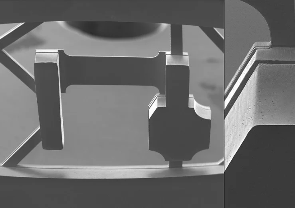
Electroforming stands out for its remarkable dimensional accuracy. Contrary to conventional manufacturing techniques, Electroforming may reach tolerances as low as ±1μm, making it perfect for creating electronic components, especially for uses where accuracy and size are crucial, such as wearable technology, drones, and consumer electronics. With Electroforming, tight tolerances, miniaturized size and volume, and consistent quality can be achieved to enhance functionality.
The Electroforming technology also excels in creating complex, multi-layer geometries that would be impossible or too expensive to produce through traditional manufacturing techniques. With multi-layer Electroforming, 3D or 2.5D structures can be achieved, including complex structures, undercuts, and internal features. This opens up the window for high-precision components that also demand delicate structures, particularly valuable in creating sophisticated electronic components that require complex internal geometries.

Another significant advantage of Electroforming technology is its high degree of customizability, particularly when combined with Laser Direct Imaging (LDI) technology. The LDI system directly translates digital designs into physical patterns on the substrate, which means no need for physical photo masks anymore. This enables engineers to easily realize complex designs and make rapid design iterations without additional costs of tooling or mask-making. Complex geometric patterns, fine details, and sophisticated features can be incorporated into the design efficiently and cost-effectively. This level of design flexibility proves invaluable in both prototyping and volume production scenarios, empowering engineers to pursue advanced component designs to make next-gen breakthroughs.
➡️ learn more about LDI technology and how it empowers Advanced Lithographic Electroforming
Furthermore, the Electroformed components exhibit superior material properties due to their fine-grain structure. This results in excellent mechanical strength, superior electrical conductivity, and an optimal strength-to-weight ratio – all critical factors in electronic device manufacturing. A variety of metals (learn more about materials used in Electroforming in details here), including copper, nickel, gold, platinum, and silver, can be used with Electroforming technology, offering flexibility in terms of electrical and thermal conductivity, corrosion resistance, and mechanical strength.
applications of Electroforming in Electronics
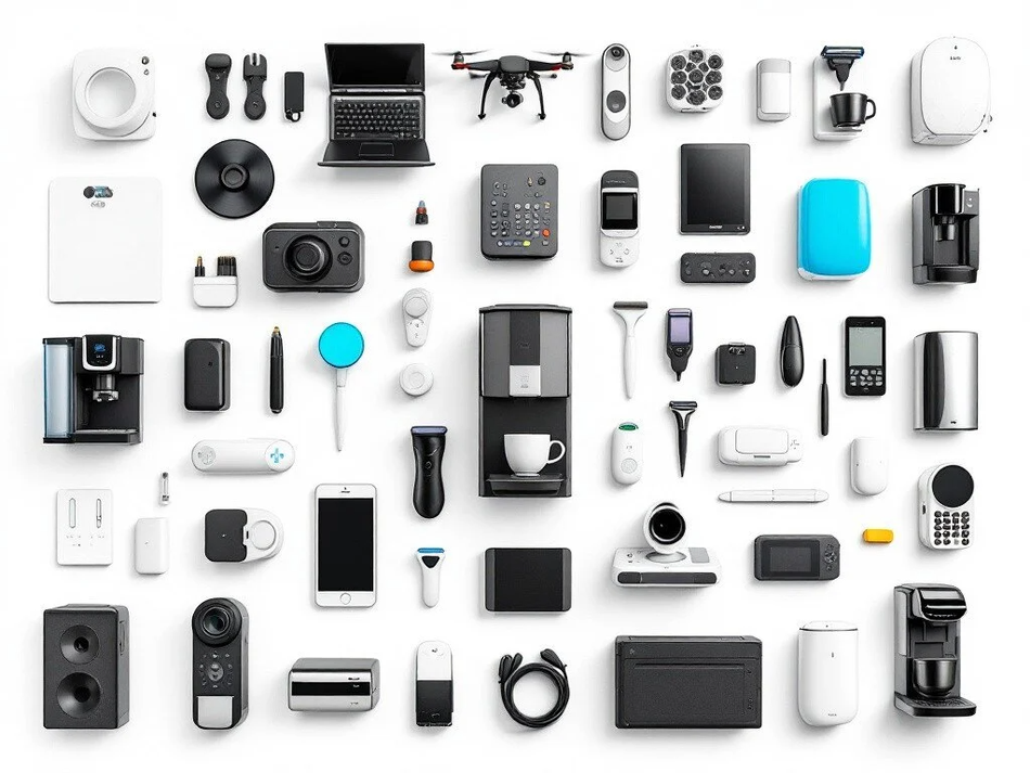
The electronics sector, where accuracy and compactness are essential, is already benefiting greatly from Electroforming. Among the applications are:
- personal care: Personal care: Ultra-thin, sharp shaver foils for high-end electric shavers are made via Electroforming, and electroplating is an option for improved cutting performance and longevity.
- inkjet printing: With Electroforming, high-quality inkjet nozzle plates with unparalleled jetting performance, superior chemical and mechanical stability can be achieved, enabling optimal printing performance.
- hearing aid components: Electroforming is the choice of technique in the production of high precision and lightweight hearing aid components, which fit within the confined spaces of modern hearing aids.
- nebulizer components: In medical electronics, electroformed components such as nebulizer plates play a vital role of controlling airflow and particle size, ensuring the effective delivery of medication.
- drones: Electroforming is used to create lightweight, high strength, high precision components such as battery foils, structural elements, micro sensor components, helping enhance flight efficiency and longevity.
➡️ learn more about applications of Electroforming
looking ahead: smaller, smarter, and greener
As the electronics industry continues the trend toward miniaturization, Electroforming's capabilities become increasingly suitable for the production of next-gen electronics components. The technology is particularly well-suited for the emerging field of wearable electronics, where components must be not only small and precise but also flexible and biocompatible. Electroforming enables the creation of ultra-thin flexible circuits, integrated antenna structures, and miniature sensor housings that can be comfortably worn on the body.
The capacity of Electroforming technology to produce intricate structures with high precision at the microscale also makes it perfect for innovative smart applications. For instance, it is also the best option for producing cutting-edge applications like components for quantum computing, micro-battery technology, and 3D semiconductor packaging.
In addition, the capability to create high-quality precision engineered components with minimal waste and 100% green energy represents a big step toward more sustainable electronics manufacturing. As industries worldwide focus on reducing environmental impact, Electroforming's highly efficient material usage and lower energy demand make it increasingly meaningful. In addition, Veco has made the transition to 100% renewable energy since 2021, obtaining 50% of its energy from solar and 50% from wind sources. This commitment to sustainability extends beyond products to the entire operational philosophy, empowering our customers and pushing boundaries of innovations in a sustainable way.

