Flip Chip Technology: Advanced Semiconductor Packaging for Next-Generation Electronics
An overview of Flip chip technology, its inception, manufacturing process, advancements and performance optimization techniques.
Introduction
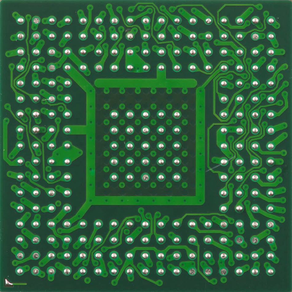
Flip chip technology represents a revolutionary semiconductor packaging method where the die is flipped and directly bonded to the substrate through conductive bumps. This advanced interconnection approach achieves superior electrical performance with parasitic inductance below 0.5 nH and resistance under 0.1 Ω. The technology enables unprecedented interconnect densities exceeding 10,000 I/Os per square centimeter, far surpassing traditional wire bonding limitations. With silicon semidconductor at its core, the flip chip technology is one of the modern innovations that promises to revolutionize the electronic manufacturing industry.
This guide provides a comprehensive technical analysis of flip chip technology's role in modern semiconductor packaging. It will explore the intricate mechanics of flip chip bonding, manufacturing processes, and performance optimization strategies. It’s an essential reading for semiconductor engineers and electronics designers seeking to maximize device performance through advanced packaging solutions.
Suggested Reading: Silicon Semiconductor: A Comprehensive Guide to Silicon and its Use in Semiconductor Technology
A Quick Historical Review of Flip Chip Technology
Flip chip packaging technology traces its roots back to the mid-20th century. While early experiments hinted at the potential of this approach, it wasn't until the 1960s and 1970s that significant strides were made.
Controlled-Collapse Chip Connection by IBM
IBM emerged as a key player in the development of flip chip technology during this era. Their groundbreaking Controlled-Collapse Chip Connection (C4) technique, which utilized solder bumps for electrical interconnections, became synonymous with flip chip packaging. This innovation laid the foundation for the technology's subsequent growth and widespread adoption.
As a result of this innovation, the modern flip chip technology has revolutionized digital design, powered by enhanced soldering techniques and advanced material sciences for:
Underfill agents
Solder material
Adhesion layers
Eventually, flip chin enhances the reliability and performance of flip chip packages. The increasing demand for smaller, more powerful electronic devices fueled the popularity of flip chip technology. Its advantages, including high-density interconnections and shorter signal paths, made it an attractive packaging solution for a wide range of applications.
Today, flip chip technology is an integral part of the semiconductor packaging landscape. It enables the miniaturization and performance enhancement of electronic devices across various industries, from consumer electronics to aerospace and telecommunications. The ongoing pursuit of smaller, more efficient, and higher-performing semiconductor packages continues to drive the evolution of flip chip technology, ensuring its relevance in the ever-changing technological landscape.
Why Flip Chip Technology is so Promising?
The direct die-to-substrate connection creates shorter electrical paths, reducing signal delays by up to 75% compared to wire bonding. Thermal resistance values as low as 0.2°C/W are achievable due to enhanced heat dissipation pathways through the bumps. The elimination of peripheral bonding enables smaller form factors, while simultaneous bump connections significantly improve manufacturing throughput.
These characteristics make flip chip technology essential for high-performance computing, 5G communications, and advanced automotive electronics where signal integrity and thermal management are critical.
Architecture and Bonding Mechanics
How Does Flip Chip Work?
Flip-chip interconnects involve attaching a semiconductor chip to a substrate using tiny copper bumps. These bumps are formed on the chip's surface and, when the chip is flipped and placed on the substrate, connect to copper pads, establishing electrical connections.
While solder balls were historically used for these interconnects, their size limitations led to the adoption of copper microbumps. Copper microbumps offer several advantages such as:
Higher I/O density
Smaller pitch sizes
Superior thermal conductivity compared to solder bumps
These benefits have solidified copper microbumps as the preferred interconnect technology for many mid-range and high-end packaging solutions.

Structural Components
The foundation of flip chip technology is its sophisticated bump metallurgy, primarily utilizing lead-free solder compositions such as Sn-Ag-Cu (SAC) alloys with precise stoichiometric ratios of Sn96.5/Ag3.0/Cu0.5. Advanced applications employ copper pillar bumps with heights ranging from 30-100μm, topped with SnAg caps for enhanced electrical conductivity and mechanical strength.
Substrate requirements demand high-density routing capabilities with line width/spacing down to 10/10μm. The substrate core typically consists of bismaleimide triazine (BT) or high-Tg FR-4 materials, with thickness variations from 0.2mm to 1.2mm depending on application requirements.
Material Type | Composition | CTE (ppm/°C) | Electrical Resistivity (μΩ·cm) | Thermal Conductivity (W/m·K) |
SAC Solder | Sn96.5/Ag3.0/Cu0.5 | 21-23 | 12-15 | 55-60 |
Cu Pillar | Pure Cu | 17 | 1.7 | 400 |
Substrate (BT) | BT Resin | 15-17 | >1E12 | 0.3-0.4 |
Substrate (FR-4) | Epoxy Glass | 14-16 | >1E12 | 0.25-0.3 |
Interconnect Design
Optimal pad layout in flip chip design requires precise geometric configurations to maximize interconnect density while maintaining mechanical stability. The fundamental pad arrangement follows an area array pattern with peripheral enhancement zones for power and ground distribution.
Critical pad-to-pad spacing must maintain a minimum of 150μm for standard applications, with advanced nodes pushing boundaries to 100μm.
Pitch specifications adhere to the fundamental relationship where the total package size (P) equals the die size (D) plus the substrate overhang (S), expressed mathematically as:P = D + S
For optimal density, the minimum pitch (Mp) follows the relationship:
Mp = Pd + 2(Bt + Ot)
Where:
Pd = Pad diameter
Bt = Bump thickness
Ot = Overlay tolerance
These mathematical relationships guide the development of high-density interconnect designs while maintaining manufacturing tolerances and reliability requirements. Current technology nodes achieve utilization rates of up to 85% in production environments.
Manufacturing Process Integration
Process Flow and Critical Parameters
The flip chip manufacturing process follows a precise sequence beginning with wafer preparation through cleaning and polishing operations. The Under Bump Metallization (UBM) process creates a reliable interface between the semiconductor die and bumps using multiple metallic layers, typically Ti/Ni/Au or Ti/Cu combinations. These layers promote optimal adhesion and electrical connectivity. The subsequent bumping technology phase employs electroplating or reflow soldering to form solder or copper bumps on the UBM surface.

Here is a detailed discussion of the flip chip manufacturing process:
Step 1: Bumping the Die
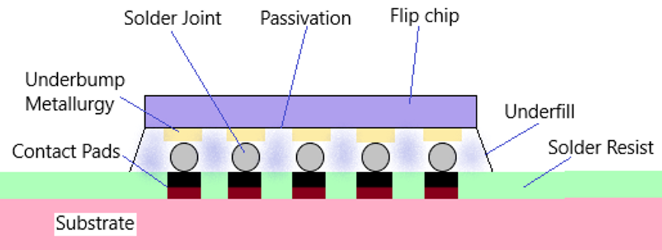
Before the chip can be attached to a substrate, tiny metallic bumps are formed on its surface. To prepare the chip for this process, a protective layer, known as the Under Bump Metallization (UBM), is applied to the connection pads. This layer shields the aluminum pads from oxidation and prevents the diffusion of metal from the solder bumps into the chip.
Next, solder material is deposited onto the UBM layer using various techniques, such as electroplating or evaporation. The solder is then shaped into spherical bumps through a process of etching and reflow.
Step 2: Attaching the Die
The chip, now adorned with solder bumps, is flipped over and aligned with the substrate. The bumps are positioned directly above the corresponding connection pads on the substrate.
The assembly is then heated in a reflow oven, causing the solder bumps to melt slightly and form strong, reliable electrical connections with the substrate pads. This process minimizes electrical resistance and inductance, ensuring optimal signal transmission.
Step 3: Epoxy Underfill
To enhance the mechanical and environmental reliability of the flip-chip assembly, an epoxy underfill is applied. This epoxy material is dispensed around the edges of the chip and flows into the gap between the chip and the substrate through capillary action.
The assembly is then cured under heat to solidify the epoxy, creating a robust bond that protects the solder bumps from moisture and other contaminants. Moreover, the underfill helps to compensate for any differences in thermal expansion between the chip and the substrate, reducing the risk of mechanical stress and potential damage.
Parameter | Measurement Unit | Description |
UBM Thickness | μm | Typical UBM layer thickness for adhesion |
Bump Height | μm | Height of solder or copper bumps |
Reflow Temperature | °C | Peak temperature during the reflow process |
Solder Paste Viscosity | Pa.s | Viscosity characteristics of solder paste |
Throughput | wafers/hour | Number of wafers processed per hour |
Die Attach Force | N | Force applied during die attachment |
Flip Chip Pitch | μm | Minimum pad-to-pad spacing in flip chip design |
Thermal profile optimization involves four critical stages in the manufacturing process. The preheat stage gradually raises temperatures to 150-200°C, preventing thermal shock. During the soak stage, temperatures maintain at 160-180°C for 60-120 seconds, enabling flux activation. The reflow stage reaches peak temperatures of 240-260°C, ensuring complete solder melting. The cooling stage requires precise control, typically at rates of 1-3°C/s, to prevent the formation of large intermetallic compounds and maintain joint reliability.
Performance Optimization
Thermal Management
Heat dissipation in flip chip packages occurs through three primary mechanisms:
Conduction through solder bumps
Convection via substrate layers
Radiation at package surfaces.
The conductive path through solder bumps provides the most efficient thermal channel, with thermal conductivity values reaching 0.4 W/(m·K) for copper bumps.
For a typical 100mm² die area with FR-4 substrate (thickness 2mm, thermal conductivity 0.25 W/(m·K)) and copper bumps (thickness 0.1mm, thermal conductivity 0.4 W/(m·K)), the total thermal resistance reaches 82.5°C/W.
Advanced cooling solutions employ multiple strategies:
Cooling Solution | Thermal Performance (°C/W) | Implementation Complexity |
Heat Spreader | 15-25 | Low |
Thermal Interface Material | 10-20 | Medium |
Microchannel Cooling | 5-15 | High |
Direct Liquid Cooling | 1-10 | Very High |
The effectiveness of these cooling solutions depends on power density requirements, with modern high-performance applications often requiring a combination of approaches to maintain junction temperatures below 85°C. Microchannel cooling systems achieve the highest cooling efficiency but require complex integration schemes and additional manufacturing steps.
Electrical Characteristics
Parasitic effects in flip chip packages are significantly lower compared to traditional packaging methods, with parasitic inductance measuring just 0.5 nH and capacitance at 0.3 pF. These minimal parasitic values enable superior signal integrity and higher operating frequencies.
Packaging Method | Signal Integrity | Parasitic Inductance (nH) | Parasitic Capacitance (pF) | Power Density (W/mm²) |
Flip Chip | High | 0.5 | 0.3 | 10 |
Wire Bonding | Medium | 5.0 | 1.5 | 5 |
BGAs | Medium | 3.0 | 1.0 | 7 |
CSP | High | 1.0 | 0.5 | 8 |
The superior electrical performance of flip chip technology enables power density capabilities up to 10 W/mm², double that of wire bonding alternatives. This enhanced power handling capability, combined with minimal parasitic effects, makes flip chip particularly suitable for high-frequency applications operating above 20 GHz.
Suggested Reading: IC Package Types: A Comprehensive Guide
Quality and Reliability Engineering
Testing and Reliability Metrics
Comprehensive flip chip quality assurance requires a multi-tiered testing approach incorporating electrical, thermal, and mechanical validation protocols. The integrated test methodology begins with electrical performance verification under operating conditions, followed by thermal cycling to assess temperature-related reliability. Mechanical shock and vibration testing evaluate structural integrity, while moisture sensitivity analysis determines environmental resilience.
Failure analysis employs sophisticated techniques for defect identification and characterization. Visual inspection serves as the initial screening method, while Scanning Electron Microscopy (SEM) provides detailed surface analysis at the microscopic level. X-ray inspection reveals hidden defects within solder joints and internal structures, complemented by electrical characterization for performance validation.
Suggested Reading: What is AOI (Automated Optical Inspection): A Comprehensive Guide
Reliability Metric | Acceptance Criterion | Significance |
Mean Time to Failure | > 1000 hours | Long-term reliability indicator |
Failure Rate | < 0.01 failures/unit | Operational stability measure |
Temperature Cycling | -40°C to 125°C | Temperature range tolerance |
Humidity Resistance | 85% RH, 1000 hours | Moisture sensitivity level |
Environmental stress testing protocols subject flip chip packages to extreme conditions to verify reliability margins. Temperature cycling tests alternate between -40°C and 125°C with 15-minute dwells at temperature extremes. Humidity testing maintains 85% relative humidity at 85°C for 1000 hours, while pressure cooker testing exposes packages to saturated steam at 121°C and 2 atmospheres. Power cycling tests evaluate thermal fatigue resistance through rapid temperature transitions under powered conditions.
Conclusion
Flip chip technology demonstrates superior electrical performance with parasitic inductance below 0.5 nH and capacitance of 0.3 pF, enabling high-frequency operations above 20 GHz. The direct die-to-substrate connection achieves thermal resistance values as low as 0.2°C/W, supporting power densities up to 10 W/mm². Critical success factors include precise control of UBM metallurgy, optimized reflow profiles maintaining temperatures between 240-260°C, and implementation of advanced cooling solutions for thermal management.
Frequently Asked Questions
1. How can parasitic inductance be minimized in flip chip designs?
Parasitic inductance reduction requires optimization of bump height (typically 30-100μm), minimizing current loop area through strategic power/ground distribution, and implementing advanced UBM structures with Ti/Ni/Au metallization.
2. What are the key process parameters for achieving optimal bump coplanarity?
Critical parameters include UBM thickness uniformity (±5%), controlled solder volume (±10%), and precise reflow temperature profile control (±2°C). Substrate warpage must be maintained below 25μm across the package diagonal.
3. What techniques optimize underfill void prevention?
Void prevention requires precise control of underfill viscosity (typically 5-10 Pa·s), optimized dispense patterns, and maintenance of substrate temperature at 80-90°C during dispensing. Capillary flow simulation models guide process optimization.
4. How are thermal cycling specifications determined for different applications?
Specifications are based on application temperature requirements plus a 20% margin. Standard automotive grade testing requires -40°C to 125°C cycling, while consumer electronics typically test from -25°C to 85°C, with dwell times calculated using thermal time constants.
References:
Table of Contents
IntroductionA Quick Historical Review of Flip Chip TechnologyControlled-Collapse Chip Connection by IBMWhy Flip Chip Technology is so Promising?Architecture and Bonding MechanicsHow Does Flip Chip Work?Structural ComponentsInterconnect DesignManufacturing Process IntegrationProcess Flow and Critical ParametersStep 1: Bumping the Die Step 2: Attaching the Die Step 3: Epoxy Underfill Performance OptimizationThermal ManagementElectrical CharacteristicsQuality and Reliability EngineeringTesting and Reliability MetricsConclusionFrequently Asked Questions1. How can parasitic inductance be minimized in flip chip designs? 2. What are the key process parameters for achieving optimal bump coplanarity? 3. What techniques optimize underfill void prevention? 4. How are thermal cycling specifications determined for different applications? References:
