
The future of data, Edge Data Center, is equivalent to a mini data centre. Its proximity to enterprises eliminates latency and other limitations, giving access to real-time data. In this article, we will delve into its core concepts, advancements, operational challenges, and real-time applications.
Be the first to know.
Get our nanotechnology weekly email digest.
Category
nanotechnology
Engineers Wiki. Most Asked Questions.
Understanding Remote I-O: An In-depth Exploration
By Umar Waseem.
16 minutes read.
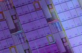
Magnetron Sputtering: A Versatile Thin Flim Deposition Technique
By Naveed Abbas.
12 minutes read.
Reactive Ion Etching: A Comprehensive Guide
By Venus Kohli.
14 minutes read.
ORGANIZATIONS. SHAPING THE INDUSTRY.


Nano Dimension
Additive Manufacturing
The ever growing need for precise micro-parts is restricted by current tech...
1 Post

Fusion Bionic GmbH
Machinery Manufacturing
We Are Giving Human Materials the Superpowers of Nature Using Lasers
1 Post

View more
TAGGED WITH 5g

Article #2 of Mastering RF Engineering: RF signal chains are key to wireless systems. Learn how components like amplifiers, filters, and mixers help plan RF designs, balance performance needs, and decide between custom-built or pre-made modules.

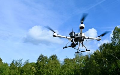
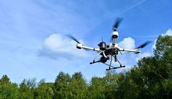
In the future, drones will take off automatically and head to an emergency scene immediately after the emergency call, transmitting initial aerial images to the emergency services control centre – even before the relevant personnel arrive.

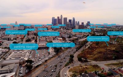
Enterprise IoT is another direction of IoT industry development, which businesses are actively adopting. Embedded technologies for large organizations bring new challenges in terms of connectivity, network stability, and data security.


This article examines whether we met the hype of 5G and where we are today with technology deployments.

Latest Posts
Reactive Ion Etching (RIE) is a powerful and versatile technique that has been widely adopted in various industries including semiconductor manufacturing, microelectromechanical systems (MEMS), and nanotechnology.
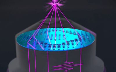
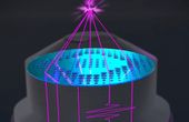
Nanofabrication technique, using holes to create vacuum guides, breaks a barrier in optics

4 minutes read

During Mobile World Congress 2023 in Barcelona, the biggest players in IoT gathered

5 minutes read


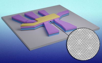
EPFL researchers have come up with a new approach to electronics that involves engineering metastructures at the sub-wavelength scale. It could launch the next generation of ultra-fast devices for exchanging massive amounts of data, with applications in 6G communications and beyond.

3 minutes read


Meet the IoT Stars community at MWC and Embedded World, and find the partners to build your next IoT Stack.
3 minutes read

A quick electric pulse completely flips the material’s electronic properties, opening a route to ultrafast, brain-inspired, superconducting electronics.
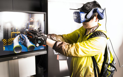
Immersive technologies and high-speed telecommunication standards are enabling new ways to work remotely.

7 minutes read


The popularity of wearable electronics has induced demand for their parts, including power sources such as triboelectric nanogenerators (TENGs). Such power sources must be both stretchy and high-performance, holding up under various deformation conditions over hours of use.

2 minutes read


In this episode, we talk about the simple, tunable machine created using common 3D printers for manipulating microscale objects to create the next generation of highly efficient antennas enabling the future of wireless communication.


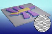
NANOWEB® is an extremely thin, transparent, conductive film that consists of an invisible, nanostructured metal mesh fabricated onto a glass or plastic surface. With its unrivaled transparency, conductivity, and flexibility, this patented functional film holds immense potential for both passive and powered use cases, with applications including electromagnetic interference shielding, antennas, 5G/6G redirection systems for elimination of dead spots, and deicing/defogging devices for vehicle windows and eyewear.


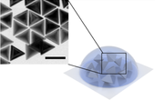
Producing chirality, a property found throughout nature, through large-scale self-assembly could lead to applications in sensing, machine perception and more.

4 minutes read

How can you spot emerging technology innovation at public companies? And how could you scale this up, so that you could track not just a handful but hundreds or even thousands of companies? For this article, I analyzed more than 650,000 financial news to find out.

9 minutes read


Announcing the December Build Month. A program to support developers in building their next IoT project with cellular technology.


Machine-to-machine (M2M) communications date back to the late 1960s. Still, it is only now that new wireless technology allows its adoption at a scale of a million devices per kilometer.

3 minutes read


Real-time monitoring of the situation in an ambulance. This provides enormous benefits for both the doctor and the patient. It could even save lives. The Connected Ambulance makes it possible.