Inkjet Printing of Solder Mask
There are three big topics that shape the production environment of today and tomorrow: digitalization, additive manufacturing, and preserving natural resources/zero waste. Learn how inkjet printing achieves these in PCB manufacturing.
25 Sep, 2023. 8 minutes read
This article was first published on
www.techblick.comAuthors:Kai Keller <kai.keller@notion-systems.com> and Lina März
This article originally appeared here.
Introduction:
There are three big topics that shape the production environment of today and tomorrow: digitalization, additive manufacturing, and preserving natural resources/zero waste.
Very tightly timed supply chains and globally distributed and connected production processes are already real and only possible because of digitalization. Additive manufacturing knocks on the door of many industrial areas, such as automotive and aerospace. Preserving natural resources and zero waste will become standard in many areas and will be the financially most convenient opportunity.
Printed circuit boards (PCBs) are manufactured mainly in Asia but distributed just-in-time all over the world. In our laptops, cars, trains, planes, TV's, audio systems, mobile phones, we all use dozens of them every day, without even realizing it. The recent stress that has been put on these supply chains also lead to investments into new facilities in North America, Europe, as well as South East Asia. So many decision makers in electronics manufacturing are currently concerned with the question which technologies they are going to use for the newly built facilities.
Today, the production process for PCBs is mainly subtractive, indicating that lots of expensive resources are wasted, are not reused, and eventually increase the costs.
This means PCB manufacturing is at home in a global, digital world but will eventually suffer from subtractive processing, waste of resources, and more complex applications and layouts.
Inkjet printing by nature is a digital technology, from image processing to discrete droplet deposition.
It is also an additive manufacturing technology. Expensive materials are only deposited where they are needed, and even the amount of material can be adjusted locally. Three dimensional structures are possible without any extra effort.
This indicates that inkjet printing is preserving resources and minimizing waste.
This article will describe the process of applying a solder mask layer by means of inkjet printing in the PCB production. It will briefly describe a PCB and outline the benefits that inkjet printing brings. This will be followed by a detailed description of the steps that were necessary to establish a stable industrial process.

Join us at TechBlick's Future of Electroncis RESHAPED conference & tradeshow in Berlin on 17-18 OCT 2023 - www.techblick.com/electronicsreshaped
Why Inkjet Printing for Deposition of Solder Mask on PCB's?
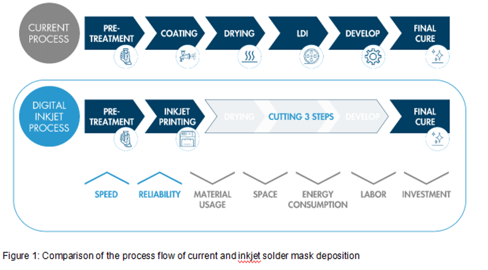
Typically, a uniform solder mask layer is deposited by a coating technology such as curtain coating or screen printing. Also, dry films are available. All have in common that they cover the whole board. After a drying step, the design is transferred onto the board via a photo mask. For each design, an own photo mask needs to be created. Alternatively, direct imaging processes with a laser are used. After illumination, the dried film is developed, and the unwanted areas are stripped and washed away. A final curing step is performed in order to achieve the full functionality. Typically, this consists of a so-called UV bump and thermal curing in a belt oven.
By summing up all the equipment needed, it's no wonder that a single production line can easily be dozens of meters long and requires a lot of staff with different skills.
The inkjet technology in contrast locally deposits the UV-sensitive material and pins it in-situ with an LED lamp. The image is loaded digitally and can be changed after each board and even be adjusted to each board individually. It is saved digitally and does not use any footprint. After the same final cure from the conventional process, the board is finished. This indicates that PCB manufacturers can drastically reduce the amount of production steps that translates in less investment cost and space for machinery and less consumption of electricity and consumables and therefore a very fast return on investment. Figure 1 shows the process flows of the conventional and the inkjet process.
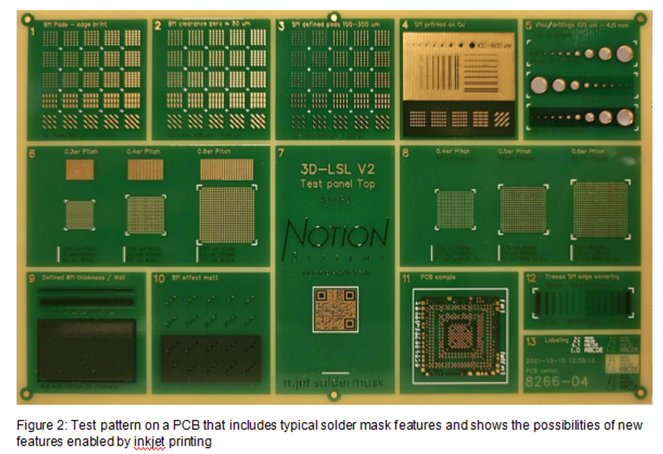
Besides, these economic and environmental aspects inkjet exclusively opens the door to a unique combination of other features that gives the PCB production industry a new level of freedom. This allows the industry to be prepared for new applications such as high frequency and 5G. Figure 2 shows an inkjet printed solder mask on a PCB and gives an overview of some unique features.
In contrast to the conventional deposition technologies, where the layer thickness is the same over the whole board, with inkjet printing, the thickness can be adjusted locally without any extra effort. There are a lot of reasons why this is beneficial for the PCB manufacturing process. Let us name three:
- Thickness zero, i.e., no solder mask where it is not required, in order to safe material or increase process stability.
- A locally adapted thickness to ease subsequent SMD assembly.
- Higher thickness at conductor or pad edges to reach higher break-through voltages.
In a summary, the main advantages are as follows:
• Digital production technology
• Additive manufacturing allows for locally adjustable thickness of layers
• New features are possible
• Labeling functions come for free
• Up to 80% less ink, as it is only print where required
• Higher yield
• Reduced space
• Reduced energy consumption
• Very fast return on investment
What Are the Requirements and What Makes Inkjet Printing of Solder Mask Tricky?
The requirements of the solder mask are defined in several norms, mainly by the IPC – Association Connecting Electronics Industries. IPC originated from Institute for Printed Circuits.
We will now describe some challenges that one faces when depositing a solder mask onto a PCB by means of inkjet printing.
First of all, the solder mask ink itself is a sophisticated material. Actually, one has to develop two materials. As an ink, it needs to have a very low viscosity, must be a Newtonian fluid, and must allow for perfect jetting in the tiny nozzles. After curing, the material needs to be extremely stable to mechanical impact and withstand harsh temperature cycles (-30 °C to +170 °C) and strong chemicals, e.g., during Ni-Au plating.
Another point is the surface. A board when it just arrives to the solder mask deposition consists of two different surfaces: the glass fiber compound (FR4) and the copper (Cu).
Join us at TechBlick's Future of Electronics RESHAPED conference & tradeshow in Berlin on 17-18 OCT 2023 - www.techblick.com/electronicsreshaped
Unfortunately, the surface energy of these areas largely differ. While the ink stays quite well on FR4, it spreads tremendously on Cu.
In addition, the height difference between FR4 and Cu can be more than 200 μm. This can have a large impact on the deposition accuracy.
Every PCB job is different. This indicates that PCBs can vary in size and thickness. Because of previous production processes, they can have bows and warpages and because of the still often manual handling even kinks. As if this was not enough, PCBs have many holes of different radii ranging from 0.1 mm up to 5 mm, of course randomly distributed over the whole area. Still, for a good performance, often absolute drop placement accuracies in the range of ± 20 μm are required. This calls for highest demands in the substrate table design and the jetting performance.
The requirements and properties of the solder resist and the printed solder resist layer are anchored in IPC-SM-840. Properties can be verified using selected test methods. The test procedure and instructions for carrying it out can be found in the test manual IPC-TM-650. Typically, the properties are divided there into visual, physical, electrical, mechanical, and chemical properties/requirements.
How to Get to Inkjet Printed PCB's
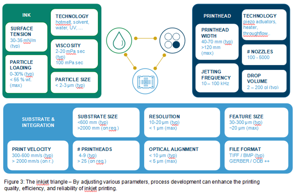
To realize the application of inkjet printing, the solder mask onto PCB's different aspects have to be taken into account, such as the choice of ink and printheads, the process development, and the machine design. Figure 3 gives an overview of typical factors that define the process and printing machine. Although the overview is generic, most of the items are relevant for the inkjet solder mask process.
The process development of each application follows the following route:
• Printhead selection
• Ink selection & material compatibility
• Waveform development
• Print process implementation
• System development (optional)
• On-site process support
It is a common misconception, especially in time-critical projects, to take the second or third step before the first. Maybe it is possible to produce a nice appearing PCB for a proof of concept, but in production, stability and more importantly predictability are crucial.
Solid results based on systematic and repeatable tests are helping to identify the process window, maximize customer satisfaction, and to reduce costly field operations.
Data Handling
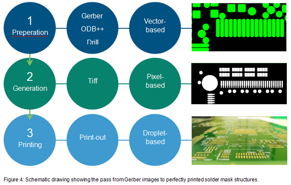
In the PCB industry, gerber is the dominating file format. Like in any other area, the conversion from vector data to discrete/digital images comes at the expense of truth to detail. Photoplotters and lasers both have this loss, but as they are operating in the range of several 10 000 of dpis, the artifacts are small. For inkjet printing, with feature sizes in the range of 30 to 80 μm and resolutions in a similar range, more care has to be taken for converting the print images.
Figure 4 visualizes the challenge. The raster image processor has to make a discrete decision based on the vector layout and the printing resolution, whether it generates a printed dot or not. For low printing resolutions, this can lead to artifacts, such as visible steps and missing dots. A high resolution would increase the level of detail but would lead to an overflow of ink or increased thickness. We have developed a conversion algorithm that considers the vector file, the real drop diameter on the substrate, and the printing resolution and adjusts the droplets in such way that the maximal level of detail can be achieved without increasing the resolution and thus not compromising throughput.
As mentioned before, conventional solder mask processes are subtractive, indicating that the full board is covered with ink and then structured. This indicates that the appearance and the geometry of inkjet-printed structures are by nature different. If one would now just use the conventional processing recipes, the result would be far from optimal. This is why, for inkjet, new design rules needed to be developed in close cooperation between technology providers, like Notion Systems and technology users, our partners, and clients. This ensures that the printed result looks more alike their conventional counterparts.
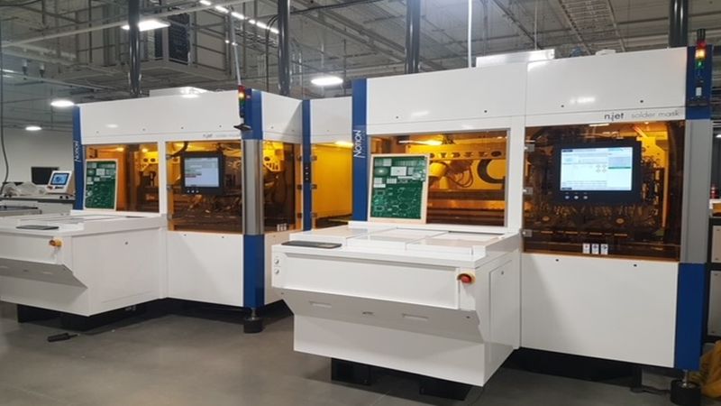
Machine Concept
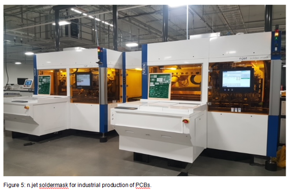
At Notion Systems, we have developed a machine concept, that is shown in Figure 5 that can be used either in manual mode or be upgraded to operate fully automated with load and unload. Our print unit covers the full substrate width with up to 20 000 nozzles, each firing more than 20 000 tiny droplets per second. The vacuum table is designed in a way that it can hold different sizes of PCBs without any mechanical clamps.
An integrated and automated non-contact cleaning system ensures that the printheads are always in good condition. The machine is easy to operate and is designed so that all important parts can be reached easily.
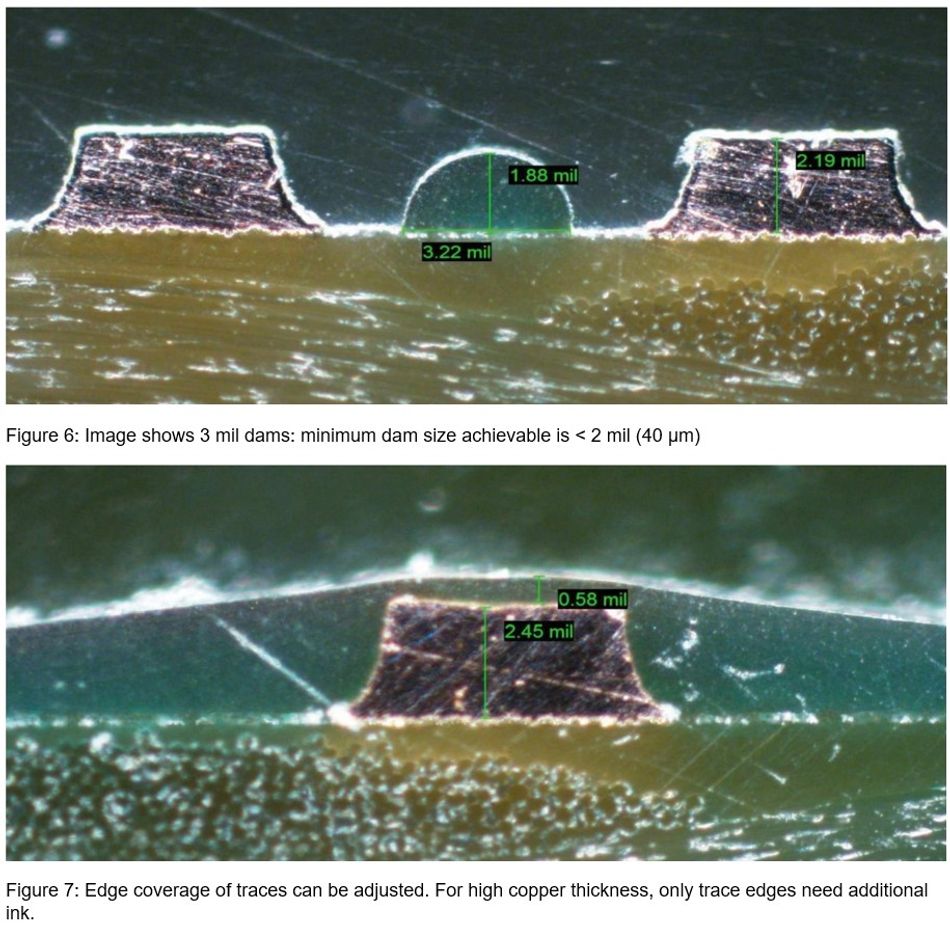
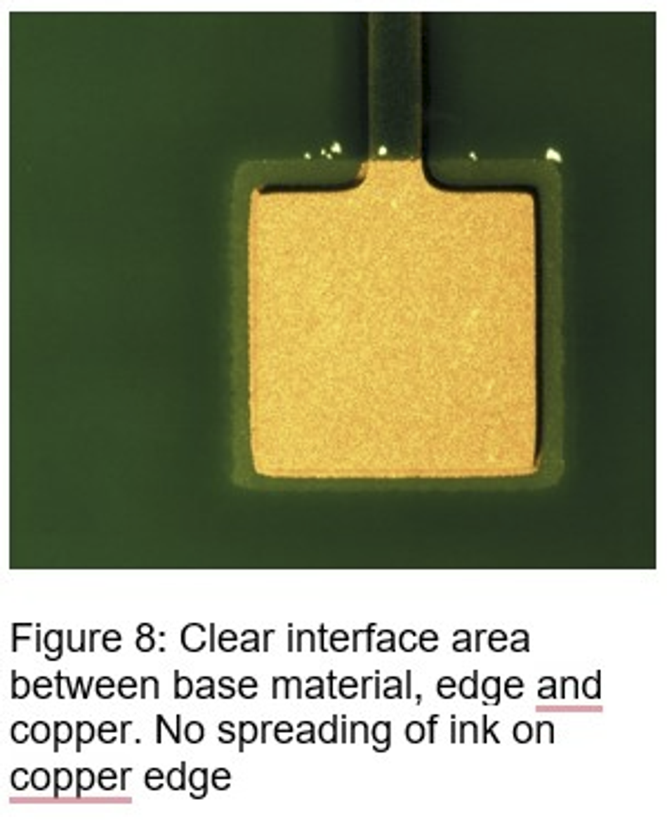
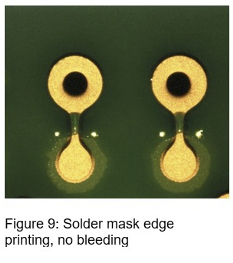
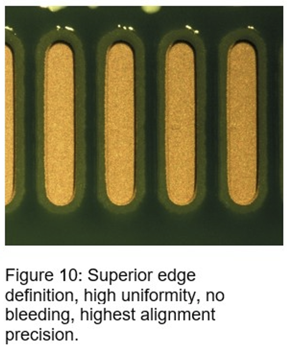
Print Images
Figures 6-10 show some examples of inkjet-printed solder masks structures. They highlight what is possible today.
Summary and Outlook
The solder mask on a PCB is perfectly suited for inkjet printing. The reduction of production steps decreases the cost and space requirements. Inkjet printing produces results that meet all requirements specified in the relevant norm for solder mask IPC 840. In addition, inkjet printing enables the implementation of useful and in its combination unique features, such as no mask in holes, locally adjusted thickness, or smart labeling.
Yet, soldermask is not the end of the story, there are many more subtractive processes in electronics manufacturing that need a closer look and possibly a replacement, if one considers what is possible with additive processes in general and inkjet technology in particular, today.