Clock Gating: Powering Down Idle Circuits
This article explores a vital power-saving technique in digital design, covering core concepts, implementations, and the differences between fine-grained, coarse-grained, and software-controlled methods. Learn why clock gating is crucial for energy efficiency, its applications in diverse systems.

17 Mar, 2025. 25 minutes read

Close-up of a digital embedded system
Key Takeaways:
Clock Gating Definition: Clock gating is a power-saving technique that selectively turns off the clock signal to portions of a digital circuit when they are not active. By preventing unnecessary clock toggling, it significantly reduces dynamic power dissipation .
Power Savings: Clocks are a major source of power consumption (often over one-third of a chip’s dynamic power). Clock gating can reduce power usage of sequential logic by an estimated 20–50% in many designs .
Implementation Techniques: Common clock gating implementations include simple AND-gate gating, latch-based gating, and flip-flop based gating. Standard cell libraries provide integrated clock gating cells (ICG) to simplify insertion of glitch-free gated clocks.
Advantages and Challenges: Clock gating yields substantial dynamic power reduction and can even save circuit area by replacing data gating multiplexers. However, designers must manage challenges like clock skew, potential glitches, and verification complexity.
Best Practices: In ASIC designs, use latch-based gating or library ICG cells and let synthesis tools automatically infer gates from clock-enable conditions. In FPGA designs, avoid gating the global clock via logic; instead use dedicated clock enable signals or specialized clock gating primitives (e.g., BUFGCE) for power reduction.
Introduction
Power efficiency is a critical concern in modern digital circuit design. Clock gating has emerged as one of the most effective techniques to reduce power consumption in synchronous circuits. The basic idea is straightforward: if a portion of a circuit does not need to operate at the moment, why waste energy clocking it? By disabling the clock signal to idle modules or flip-flops, clock gating eliminates unnecessary switching activity, thereby cutting down dynamic power usage. This technique is widely used—from individual register banks to large functional units and even entire subsystems—making it a cornerstone of low-power digital design.
The motivation for clock gating becomes clear considering the role of clock networks in power dissipation. The clock signal in a chip toggles at the highest frequency and typically drives a vast number of gates and flip-flops. In many ASICs and SoCs, the clock distribution network alone can account for a huge fraction of the dynamic power (commonly 30–50% of total switching power). If we can stop the clock from toggling parts of the circuit that don’t need to switch, we can save a proportional amount of power. In fact, clock gating is known as a “tried-and-true” power reduction method, often yielding 20–30% dynamic power savings for sequential logic blocks with no impact on functionality .
This article covers various gating techniques, and practical HDL coding and EDA tool usage. It discusses power and area advantages, alongside challenges like skew and verification. Best practices for ASICs and FPGAs are provided, with industry examples and future trends explored. Clock gating is crucial for low-power design, complementing techniques like power gating and voltage scaling.
Suggested Reading: ASIC vs FPGA: A Comprehensive Comparison
What is Clock Gating?
Clock gating is a power management technique used in synchronous digital circuits to reduce dynamic power consumption by selectively stopping the clock signal for portions of the circuitry that are not actively switching. In a normal synchronous design, the clock continuously toggles flip-flops and sequential elements every cycle, even if a particular subsystem or register is idle or holding a constant value. This constant switching consumes power without performing useful work.
Clock gating “prunes” the clock tree by disabling the clock input to idle circuits, so that the flip-flops in those sections do not receive the clock and thus do not toggle. When the clock is stopped for a given section, the flip-flops hold their state (no state changes occur) and the only power they consume is leakage (static power), which is usually much lower than dynamic switching power.
In essence, clock gating inserts a small logic circuit into the clock path of a register or block. This gating circuit can turn the clock on or off to that part of the design based on a control condition (often an enable signal). If the control indicates the block is idle or its state need not change, the gated clock is held at a steady level (no transitions), effectively pausing all sequential activity in that block.
When the block needs to become active again, the gate re-enables the clock, resuming normal operation. From the system’s perspective, the functional behavior is the same as if the block were continually clocked (assuming the gating control is designed correctly), but during idle periods, power is saved by not clocking it.
Why Is Clock Gating Needed?
Switching power is a dominant component of power dissipation in CMOS circuits when active. Every toggle of a flip-flop’s clock input causes internal transistors and loads to charge or discharge, consuming energy. By eliminating toggles when they are not needed, we eliminate that energy usage. The power savings can be substantial, especially in large designs where many units often remain idle waiting for work. Modern processors and SoCs employ aggressive clock gating at many levels. For example, functional units (like multipliers, ALUs, caches) may be clock-gated when not in use, entire peripheral IP blocks may be gated when disabled, and even pipeline registers can be gated during pipeline stalls.

This pervasive use of clock gating is one reason why contemporary chips can achieve high performance yet stay within power and thermal limits.
Suggested Reading: Linear vs Switching Power Supply: Understanding the Differences
To put it in perspective, consider that “more than one-third of an IC design’s dynamic power is in the clock-distribution system”, as noted in a classic low-power design discussion. If you can shut off clocks to parts of the chip whenever they aren’t needed, it’s essentially free power savings. Indeed, using an enable signal to control a clock gating cell for a group of registers can save around 20–30% of the dynamic power of those sequential elements with no performance loss. Clock gating has become so standard that design tools often automatically insert clock gating based on RTL coding styles.
Types of Clock Gating Techniques
There are several techniques to implement clock gating in hardware, each with its own circuit structure and trade-offs. The goal of all these techniques is the same – stop the clock from reaching certain flip-flops when not needed – but the methods differ in how they achieve a glitch-free and safe gated clock. The three common types of clock gating implementations are:
AND-gate based clock gating (simple combinational gating)
Latch-based clock gating (using a level-sensitive latch to avoid glitches)
Flip-flop based clock gating (using an edge-triggered flip-flop or specialized cell for gating control)
After describing each, we will compare these techniques in terms of simplicity, safety, and usage.
AND-Based Clock Gating (Combinational Gating)
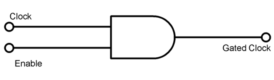
The most straightforward way to gate a clock is to use a basic logic gate (AND or OR) to combine the clock with an enable signal. For example, consider an AND gate used to gate the clock: one input is the original clock, and the other input is an active-high enable. The output of the AND gate is the gated clock that goes to the target flip-flops. When the enable is 1, the AND gate passes through the clock pulses to the flops; when the enable is 0, the AND gate outputs constant 0, effectively holding the clock line low (no toggles reaching the flops). This simple scheme is illustrated by a basic diagram of an AND gate gating a clock signal.
Similarly, an OR gate with an active-low enable (driving the OR gate input to 1 to stop the clock) can be used for clock gating– the concept is analogous .
Advantage: The AND-gate gating approach is very simple and involves minimal additional hardware (just a single gate). It directly implements the intuitive idea of “clock = clock AND enabled”. In terms of logic, it doesn’t get simpler than this.
Main drawback: This naive approach can introduce glitches on the gated clock if not used carefully. The problem arises because the enable signal might change state at arbitrary times relative to the clock transitions. If the enable input to the AND changes while the clock is high, it could create a short spurious pulse or cut off part of a pulse – a glitch – on the output clock line. For example, suppose the clock is high and the enable goes from 1 to 0 slightly after the clock’s rising edge; the AND gate might output a short high pulse that doesn’t align with the proper clock edges.
Latch-Based Clock Gating (Glitch-Free Gating)
To avoid the glitch problem of simple gating, practical clock gating circuits incorporate a level-sensitive latch (or equivalent mechanism) to synchronize the enable signal with the clock. The idea is to ensure that the enable control only changes at a time when the clock is in a stable phase (e.g., when the clock is low, if gating a positive-edge clock). By capturing the enable in a latch transparent during the inactive phase of the clock, we guarantee that when the clock goes high (active edge), the gating control is held steady, preventing any mid-cycle changes.
A common implementation is to use a low-level sensitive latch on the enable signal in conjunction with an AND gate for gating a positive-edge triggered clock Here’s how it works: When the clock is low, the latch tracks the enable input; when it goes high, the latch freezes, providing a stable enable for the AND gate. This ensures the gated clock is either a clean replica or fully suppressed during the high phase, preventing glitches.
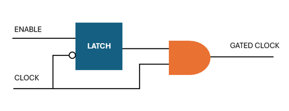
This latch-plus-AND structure is commonly called a glitch-free clock gating circuit. It yields what we want: when enable = 1, the output clock toggles in sync with the input clock; when enable = 0, the output clock remains low (or if using OR gating with active-low enable, remains high) throughout. The clock enable signal is effectively sampled on the falling edge of the clock, and the decision to pass or block the next rising edge is made cleanly . Many references show this as the standard solution – for example, “the output won't be glitchy if the enable signal changes only when the CLOCK signal is low... ensure the enable is generated by a negative-edge-triggered FF or latch” . The result is a glitch-free gated clock as required.
Advantages: Latch-based gating safely produces a gated clock that is free of glitches, which is crucial for reliable operation. This technique is the de-facto standard in ASIC flows and most digital libraries offer a pre-designed cell that internally uses this latch+AND (or latch+OR) combination. Another benefit is that a latch-based gating cell can be shared by multiple flip-flops that use the same enable, gating an entire group with one control, which is area-efficient.
Considerations: The latch-based approach introduces a small additional latency in gating response – effectively, the enable is sampled on a clock edge, so gating or ungating can be quantized to clock cycles. Also, the gating logic itself (latch and gate) adds a small propagation delay in the clock path, which must be accounted for in clock tree design (more on that in challenges).
Flip-Flop-Based Clock Gating
Flip-flop-based clock gating is conceptually similar to latch-based gating, in that it uses a storage element to hold the enable during the critical portion of the clock cycle. Instead of a level-sensitive latch, this technique might use an edge-triggered flip-flop (FF) to synchronize the enable to the clock, or a specialized pulse generator. One approach is to capture the enable on the falling edge of the clock with a flip-flop, and then feed that into an AND/OR gate with the clock.
This is effectively the same behavior as the latch method (since a flip-flop triggered on the negative edge will update the enable at clock low and hold it during clock high). In practice, the difference between using a negative-level latch vs. a negative-edge flip-flop for gating control is minor – both aim to prevent changes during the clock high phase. The latch is often preferred in custom cells for its simplicity (fewer transistors than a full flip-flop), but a flip-flop can do the job too.
Another interpretation of “flip-flop-based” clock gating is using integrated flip-flops with built-in gating. Some sequential elements are designed to internally gate their clock when an enable is inactive.
In FPGAs, for instance, every flip-flop inherently has a clock enable input . When you use the clock enable on an FPGA flip-flop, the FPGA’s hardware essentially ensures the flip-flop does not toggle its state if the enable is false (it typically implements this by a mux in front of the FF or by gating the clock to the storage element internally). From the designer’s perspective, it’s as if the flip-flop “skips” clock pulses when disabled. In ASIC libraries, there are also multi-bit flip-flop structures or specialty flops that can do conditional capture, but generally the library approach is to use separate gating cells.
Suggested Reading: FPGA vs. Microcontroller: Understanding the Key Differences
Advantages: Flip-flop based gating (in the sense of synchronizing the control via a flop) is also glitch-free. It can be easier to integrate using existing flip-flop components (especially in FPGA contexts or certain standard cell offerings). For FPGAs, using the provided clock enable is absolutely the safest and recommended way to achieve clock gating behavior (more on FPGA specifics later).
Considerations: Using a flip-flop or latch for gating control achieves synchronous operation, preventing glitches. In ASICs, library cells (ICGs) abstract these implementations, making "latch-based" and "FF-based" gating functionally equivalent. These "clock gating cells" ensure safe clock transitions via stored enables, simplifying design and preventing glitches.
Comparison of Clock Gating Techniques
Each clock gating method has pros and cons. The following table summarizes the differences:
Clock Gating Technique | Implementation | Pros | Cons / Considerations |
AND-based gating | Combinational gate (AND/OR) directly on clock with enable. | Very simple – minimal logic needed. | Glitch-prone if enable changes during clock high; not safe unless enable is guaranteed synchronized. Rarely used standalone due to hazard risk. |
Latch-based gating | Level-sensitive latch (e.g. transparent when clock=low) feeding an AND/OR gate. Often provided as an integrated cell. | Glitch-free clock output (safe gating). Widely used in ASICs via ICG cells. | Slight clock path delay and area overhead (latch + gate). Enable is sampled, introducing one clock-cycle latency for on/off. |
Flip-flop-based gating | Edge-triggered flip-flop synchronizing enable, then gating logic (similar to latch method). In FPGA, use of built-in clock enable or BUFGCE. | Glitch-free (synchronized control). Leverages existing flip-flop features (FPGA clock enables). | Similar overhead to latch method. In ASIC flows, usually realized with dedicated gating cells rather than discrete FF+gate. In FPGAs, gating the global clock is limited to special buffers (BUFGCE) and not as power-effective as in ASIC (discussed later). |
Clock Gating Implementation in Digital Circuits
Implementing clock gating in a design can be done at different levels of abstraction: in the RTL code (HDL), using library cells in a schematic or netlist, or via EDA tool automation during synthesis. This section covers how designers specify clock gating and how tools realize it.
RTL Coding for Clock Gating (Using Clock Enables)
In RTL (Register-Transfer Level) design using languages like Verilog or VHDL, designers typically do not explicitly instantiate an AND gate on the clock. Instead, they code their sequential logic using clock enable conditions, and then allow the synthesis tools to convert those into gated clocks if appropriate. For example, consider a simple RTL code snippet in Verilog:
always @(posedge clk) begin
    if (enable)
        Q <= D;
    else
        Q <= Q;  // hold the previous value
end
This describes a flip-flop that loads a new data D on each rising clock edge only when enable is true; otherwise, it retains its old value (Q <= Q). In hardware, one way to implement this behavior is to use a multiplexer on the D input (when enable=0, feed back Q, effectively not changing state).
Synthesis tools can automatically implement clock gating, recognizing patterns like mux feedback flops and replacing them with gated clock constructions. Designers typically use if (enable) in RTL, allowing the tool to infer and optimize clock gating by sharing cells among multiple flip-flops with the same enable. This reduces power and area by replacing numerous muxes with a single gating cell.
RTL designers should code using enables and let synthesis tools handle gating, ensuring the tool's clock gating optimization is enabled for ASICs. Manual instantiation of clock gating cells is possible for specific cases, guaranteeing gating but reducing RTL genericity. Intent-based clock gating, where tools infer gating from RTL patterns, is often preferred over tool-inserted gating.
Clock gating reduces die area and power by replacing muxes with efficient gating logic. Synthesis replaces mux+flop combinations with gated clocks, reducing power and area. This is because a single gating cell can control multiple flip-flops, replacing numerous muxes.
Clock Gating Cells and Library Support
ASIC standard cell libraries include specialized clock gating cells (ICGs) that encapsulate glitch-free gating logic. These cells, with inputs for clock and enable, provide a characterized, optimized gating function, ensuring consistent timing and power performance.
When a synthesis tool inserts clock gating, it will use these library cells. The example transformation earlier would replace a group of flip-flops and their common enable logic with one instance of an ICG cell (driven by that enable) feeding the clock of those flops. This inserted cell counts toward the design’s sequential cells (it’s effectively like adding a latch), and it must be handled in downstream flows (placement, clock tree synthesis, verification, etc.). Designers can also manually instantiate these cells in their RTL if they want explicit control.
During Clock Tree Synthesis (CTS), clock gating cells are integrated into the clock network, and their insertion delay is accounted for. Static timing analysis (STA) ensures enable signals meet setup and hold times, preventing latch timing violations. STA typically constrains enable changes to the clock's low phase, guaranteeing glitch-free operation. Proper timing constraints, as specified in library files, automate this process.
Design Automation Tools for Clock Gating
Modern EDA tools provide strong support for clock gating, both at the synthesis stage and for verification. Here are some aspects of tool support:
Automatic Gating in Synthesis: As mentioned, tools like Synopsys Design Compiler (with Power Compiler), Cadence Genus, or Mentor (Siemens) support automatic clock gating insertion. The user can typically enable a parameter for this optimization. The tool will identify registers that have an explicit or implicit enable condition. Often, groups of flip-flops driven by the same enable are gathered so that a single gating cell can control them all. This grouping maximizes power savings while minimizing added cells. Synthesis will output a report (often called a “clock gating report”) detailing how many gating cells were inserted and which registers were gated. Designers should review this to ensure critical parts are gated as expected. There might be cases where the tool decides not to gate something (e.g., if the enable condition is not readily apparent or if gating a single flop isn’t deemed worthwhile).
RTL Clock Gating vs. Gate-level Insertion: Some flows allow clock gating insertion at the gate level or during an optimization phase. However, doing it at RTL or during synthesis is more common and easier to manage. One should avoid manually editing gate-level netlists to add gating, as that is error-prone – use the automated features or code it in RTL.
Clock Gating Verification: Functional verification needs to ensure that when a clock is gated, the system still behaves logically correct (e.g., the gated block truly didn’t need to change state during that period). Equivalency checking tools (formally verifying that the gated implementation matches an ungated specification) are typically used. Also, specialized formal checks can verify that no clock domain crossing issues are introduced (a gated clock is essentially a conditional clock domain; one must ensure, for example, that data launched on a gated clock is not captured by another clock domain without proper synchronization).
Low-Power Intent (UPF/CPF): In advanced flows, designers might employ power intent languages like UPF (Unified Power Format) or CPF. These allow specification of power domains, which can include clock gating strategies or retention strategies. While UPF is more often used for power gating and multi-voltage design, one could envision using it to specify certain clocks are gated under certain conditions. However, since clock gating is so integrated with logic, it’s typically handled at RTL rather than separately in UPF.
Physical Implementation: Placement of clock gating cells is done carefully. They are part of the clock path, so they are often placed in the vicinity of the flops they control to minimize skew. The physical design tools and CTS ensure that any skew introduced by gating is balanced. There are also techniques like clock gating clusters – grouping flops around a gating cell physically to optimize the local clock distribution.
Advantages and Challenges of Clock Gating
Clock gating offers clear benefits for power reduction, but it also comes with certain challenges and trade-offs. Let’s break down the advantages first, and then the challenges (or potential drawbacks) that engineers must manage.
Advantages of Clock Gating
Significant Dynamic Power Reduction: Clock gating significantly reduces dynamic power by preventing unnecessary clock toggling, yielding substantial power savings, often double-digit percentages. This directly translates to less heat, extended battery life in portable devices, and reduced active current draw. Gated clocks can save 20-30% of switching power in sequential blocks, with some achieving over 50% reductions. These benefits provide performance headroom and help meet tight power budgets.
Reduced Effective Capacitance Load: By gating off sections of the clock tree when not in use, the effective capacitance being driven by the root clock is reduced during those periods. This means the clock source (PLL or global buffer) also sees a lighter load at times, which can further save power. In effect, you are dynamically trimming the clock tree. One might say clock gating improves energy proportionality – power usage scales more closely with actual usage of different blocks.
Lower Toggle Noise and EMI: With fewer transitions, there’s less simultaneous switching noise and potentially less electromagnetic interference generated by the chip. Clock signals switching cause current spikes; gating some of them off moderates these spikes. This can improve supply noise margins and reduce di/dt stress on power distribution.
Minimal Performance Impact: Clock gating, when properly implemented, does not impact the functional performance or clock frequency of the design. The circuit still runs at the same clock speed when enabled; gating only pauses the clock when you weren’t doing useful work anyway. So from a throughput perspective, you lose nothing (except the rare case where gating adds one cycle latency when re-enabling, which is usually negligible or planned for in control logic).
Area Savings by Replacing Data MUXes: An often overlooked benefit is that clock gating can sometimes reduce circuit area compared to alternative gating via data-path multiplexers. If a design uses a lot of clock-enable style registers (with input muxes for hold behavior), replacing those muxes with a shared clock gating cell can cut down on logic duplication. As noted earlier, removing numerous 2:1 multiplexors on flip-flop inputs and using one gating cell is more area-efficient for a group of registers.
Heat and Thermal Benefits: Reducing power means less heat generation. Gated clocks can keep a chip running cooler, which in turn can improve reliability and potentially allow for more aggressive performance in other areas (since thermal limits are less strained). Especially in scenarios like ASICs in smartphones, where certain subsystems (e.g., DSP or radio blocks) are gated when not needed, the temperature and battery life benefits are tangible.
Suggested Reading: Thermal and Heating Solutions for Printed Electronics
Challenges and Potential Drawbacks of Clock Gating
Despite its benefits, clock gating does introduce some complexities and requires careful design. Key challenges include:
Clock Skew and Timing Impact: Gated clocks introduce phase delays, causing skew between gated and ungated clock domains, potentially leading to timing violations. Clock Tree Synthesis (CTS) addresses this by treating gating cells as sinks, balancing clock trees, and accounting for their propagation delays. Designers use constraints to ensure proper timing, effectively integrating gating cells into the launching path for downstream flip-flops. This ensures synchronized clock edges across the circuit, mitigating skew-related timing issues.
Glitch-Free Requirement: Gated clocks must be glitch-free, ensured by using standard gating cells and meeting timing requirements. Improper gating signal control leads to catastrophic glitches. To prevent this, enable signals must adhere to clock gating setup/hold times, typically requiring synchronization with the clock. Asynchronous or randomly timed signals must be synchronized before being used for gating.
Verification Complexity: Gated clocks complicate simulation and verification due to circuit sections turning on and off independently. Verification must confirm intended constant register values during gated-off periods and ensure proper resumption after re-enabling. Scenarios involving handshakes across gated boundaries and independent clock gating interactions must be thoroughly tested. Verification teams create specific scenarios to cover these conditions, ensuring robust functionality.
Design and Architectural Complexity: Deciding where and how much to gate requires architectural thinking. If you “over-gate” (gate too many fine-grained things or in a design with very few idle cycles), you might add unnecessary complexity for little gain. Each gated domain might need additional logic to control the gating (e.g., a control FSM that knows when to stall a pipeline stage). These additional conditions add to design complexity and verification overhead. As a guideline, gating is most beneficial when there are significant periods of inactivity or when a large group of registers share an inactivity condition. If a design toggles almost every cycle, gating might not find many opportunities (and the gating logic itself would consume power).
Area and Power Overhead of Gating Logic: Gating cells consume power and area. Fine-grained gating, like one cell per flip-flop, may not be efficient due to this overhead. Tools use heuristics to avoid gating low-toggle-rate flops, favoring coarse enables for multiple flops. While area overhead is typically small compared to power savings, it's not negligible. Determining the optimal gating granularity is crucial; engineers often start with block-level gating for significant gains, then assess smaller group gating as needed.
Clock Domain Crossing (CDC) and Design Constraints: A gated clock is effectively a conditional clock domain. If other logic interacts with a block that has a gated clock, designers must ensure proper synchronization when that block’s clock is stopped. Generally, if a block is truly idle when gated, it shouldn’t be sending or receiving data; but if there are signals crossing in/out, you have to ensure they don’t cause issues when one side is paused.
Best Practices for Implementing Clock Gating in ASIC and FPGA Design
Implementing clock gating effectively requires adhering to certain best practices in design and verification. These practices differ slightly for ASICs vs. FPGAs due to the inherent differences in how clocks are handled in those domains. Below, we break down recommendations for each:
ASIC Design Best Practices for Clock Gating
Plan Gating Early and Use a Coherent Strategy: As part of the initial microarchitecture or power architecture, decide which modules or registers will be clock-gated. Identify idle scenarios (e.g., a cache when not accessed, a bus interface when inactive, etc.) and specify the conditions under which clocks can be turned off. Early planning allows the RTL to be written with the necessary enable signals and ensures that any required handshakes or flush mechanisms are in place.
Leverage Synthesis Inference: Write RTL using enable signals for registers that can idle, as described earlier, rather than manually gating clocks via gate instantiations in the code. Allow the synthesis tool to infer clock gating for these registers. Synthesis tools are quite good at identifying common enables and inserting gating cells.
Use Integrated Clock Gating (ICG) Cells: Always use the library’s provided gating cells (or a cell combination recommended by the library) instead of crafting custom gating logic from basic gates. The library cells are characterized for short latency and glitch-free operation. When instantiating an ICG cell manually, ensure you tie any control pins properly (some cells have a second enable for test modes or scan-disable, which might need to be tied off or controlled via test logic).
Gating Control Signal Generation: Design the logic that generates the gating enable carefully. Ideally, the gating control should be generated from flops clocked by the same clock (or a safe synchronized domain). For example, if you have a “block_idle” signal that goes into a gating cell’s enable, that block_idle should itself come from synchronous logic (like a small FSM that observes the block’s state). This ensures the enable only toggles in sync with the clock.
Group Signals and Avoid Over-Gating: It’s often better to use one gating cell for a group of related registers (that share an enable) than to have many tiny gated domains. Grouping improves gating efficiency. Avoid gating signals that toggle frequently or for very short idle periods, as the overhead may not be worth it. A common practice is to not gate if the duty cycle of activity is above a certain threshold, or if the number of flops under an enable is small.
Observe Clock Gating Timing Checks: When running static timing analysis, always pay attention to clock gating checks. Ensure that no violations exist for gating setup/hold on the enable pin of gating cells. If you find a violation, it means the enable is changing too close to the active clock edge. The fix might involve adding one pipeline stage to delay gating or tightening logic so that condition is ready earlier. These constraints are critical to guarantee glitch-free clocks.
Verification and Simulation: Simulate various scenarios of the gating logic. For example, simulate a scenario where a block becomes idle and ensure the enable goes low, then see that the block’s internal signals stop toggling (power simulations or annotations can help visualize power reduction). Use assertions if possible: e.g., an assertion that if clock_enable is low, then certain outputs remain stable. Also verify the wake-up: when enable goes high again, the block should resume seamlessly. If using power-aware simulation tools (with UPF), you can simulate gated clocks effect (some simulators can gate clock events). Additionally, consider formal verification to prove that gated vs non-gated design are equivalent under the intended conditions.
Synthesis and Physical Implementation Settings: Work with the backend team (physical design) to ensure they are aware of which clocks are gated. The CTS tool might need guidance, for example, which gating cells are the sync points. Some flows treat the output of a gating cell as a new “generated clock” that needs constraints. Make sure those are set so that timing is analyzed.
Test Mode Considerations: Many designs include a way to bypass or disable clock gating during scan test or debugging, to ensure full controllability of flops. Gating can interfere with scan chains if, for instance, a scan capture is expected but the clock is gated off. To handle this, gating cells often have a “test enable” override or the design uses OR gates to force enables during test mode. Ensure that in test mode (scan mode), all clock gating either is transparently ON or properly controlled. Check coverage of scan patterns to ensure gated flops can still toggle when needed for test.
FPGA Design Best Practices for Clock Gating
Clock gating in FPGAs needs special attention because FPGAs have a fixed, global clock distribution architecture that does not always allow arbitrary logic gating without consequences. Some guidelines for FPGAs:
Use Clock Enables Instead of Gating Logic: The golden rule in FPGA design is do not gate the clock signal with LUTs or random logic. Unlike ASIC, inserting a combinatorial gate on an FPGA clock can wreak havoc on timing (introducing unpredictable skew) and may prevent the clock from using the low-skew global routing resources. Instead, use the dedicated clock enable (CE) input that each flip-flop in the FPGA fabric provides . Writing RTL with if (enable) Q <= D; else Q <= Q; as shown earlier will infer use of the flip-flop’s CE line, not a gated clock. The flip-flop’s internal circuitry ensures that when CE is low, the flip-flop ignores clock edges (i.e., it doesn’t change state). The clock still toggles throughout the FPGA, but at least the logic downstream doesn’t toggle, saving some power in the logic slices.
Leverage Dedicated Clock Gating Primitives (BUFGCE/BUFHCE): Many FPGA families provide dedicated clock gating or clock enable primitives on the global/regional clock buffers. Xilinx FPGAs have BUFGCE (global clock buffer with clock enable) and BUFHCE (half-region buffer with enable). These are essentially built-in glitch-free gating elements at the distribution level. If you truly need to shut off a large portion of the FPGA’s clock tree to save power (for instance, turning off a whole region of logic), you should use BUFGCE rather than an LUT gate.
Timing Closure for Gated Clocks: If you use clock gating in FPGA (via BUFGCE or similar), be mindful of clock domain crossings. A gated clock output from BUFGCE is usually treated as a separate clock domain by static timing (because it can stop/start). If the design has signals crossing from a gated clock domain to another, you should constrain them properly (false path or multi-cycle as appropriate, or use handshake synchronizers). The FPGA timing analyzer will also report skew between a gated clock domain and an always-on clock domain. Typically, one should avoid high-speed data transfers between a gated clock region and another without synchronization, or simply design so that the gated domain can pause without affecting others (like isolate it).
Glitch-Free Design Techniques: The FPGA tools enforce that the enable for BUFGCE comes from a flip-flop (they often require the CE to be synchronous to avoid glitches on enable). Still, as a designer, ensure that you drive BUFGCE enable from a registered signal (in the same clock domain you are gating).
Power Estimation and Measurement: Use FPGA power estimation tools (Xilinx Power Estimator, Intel Power Analyzer, etc.) to quantify the benefit of your gating strategy. These tools can simulate how much power is saved when certain regions are clock-gated or when certain flip-flops use clock enables. Because FPGAs have a significant static power and clock distribution overhead, the measured savings might be smaller in percentage terms. Still, any reduction in unnecessary toggles helps, especially for cooling or battery-operated FPGAs. Measure power with designs with and without gating to see if it’s worthwhile; for some FPGA designs, it might only matter in very power-sensitive contexts.
Alternative Low-Power Techniques: Since aggressive clock gating is not as straightforwardly beneficial in FPGAs (you can’t, for example, gate the entire chip’s clock easily without just stopping the clock input which is akin to a sleep mode), consider alternative or complementary techniques. For instance, use power gating hard blocks (some FPGAs allow powering down certain blocks like transceivers when not in use).
Don’t Violate Tool Guidelines: FPGA vendor documentation often explicitly states: “Remove LUTs or any combinatorial logic in clock paths as they make clock delays and skew unpredictable during placement”. Adhering to this, never try to DIY a clock gate by ANDing a clock with a signal in the fabric LUT – this will produce a huge skew (because that LUT will be placed somewhere not aligned with global clock buffers) and likely cause hold time or routing issues. The FPGA place-and-route might even convert it to a high-skew net or issue a warning “clock net is gated by logic”. Always use the dedicated resources or the flip-flop CE method.
Use Clock Domains Wisely: In FPGAs, sometimes using a separate clock domain that you can completely stop is an option. For example, if you have a portion of the design that can be entirely shut off, you might drive it with a separate clock that you can disable at the source (e.g., through an MMCM or clock generator gating feature). Stopping a secondary clock domain’s source (like disabling a PLL output) can be seen as an extreme form of gating (actually it’s more like stopping the clock at the source).
For FPGAs, prioritize flop-level clock enables and vendor-provided primitives for coarse gating. Direct clock gating within FPGAs offers minimal power savings due to the fixed global clock tree. Focus on architectural low-power strategies rather than mimicking ASIC gating.
Suggested Reading: FPGA Design: A Comprehensive Guide to Mastering Field-Programmable Gate Arrays
Conclusion
Clock gating significantly reduces dynamic power in digital circuits by selectively disabling clocks to idle portions. Effective techniques, including latch-based gating, prevent glitches. Modern designs leverage synthesis tools and dedicated cells for safe, skew-minimized implementation in ASICs and FPGAs. Benefits include substantial power savings with minimal overhead, but challenges exist in managing skew, glitches, and verification.
Best practices involve using enables, library cells, and synchronizing controls. Industry examples demonstrate significant power reductions through smart gating. Future trends point towards more automated and fine-grained gating, essential for meeting stringent power budgets in modern electronics. Mastering clock gating is crucial for designing energy-efficient hardware, requiring a blend of theoretical understanding and practical implementation.
FAQ
Q1: What is clock gating and why is it used?
A1: Clock gating is a technique in digital circuit design where the clock signal to certain flip-flops or modules is turned off (gated) when those parts of the circuit are not needed. It is used to reduce dynamic power consumption. Normally, clocks toggle continuously and consume power even if a circuit’s state isn’t changing. By gating the clock, we prevent those toggles, thereby saving the power that would have been wasted on unnecessary switching . In summary, clock gating stops the clock for idle circuitry, which significantly cuts down switching power while maintaining the circuit’s state.
Q2: How does clock gating differ from power gating?
A2: Clock gating reduces dynamic power by disabling clocks to idle circuits, stopping toggling while keeping them powered. Power gating reduces static power by cutting off power to unused blocks, eliminating both switching and leakage currents, but losing state. Clock gating is lighter, instantly resuming; power gating saves more but has state loss and longer wake-up. Designers combine them: clock gate for brief idleness, power gate for longer periods.
Q3: What are the main techniques to implement clock gating?
A3: The main clock gating implementation techniques are:
Combinational gating (AND-gate gating): Using an AND/OR gate to directly gate the clock with an enable. This method is simple but can cause clock glitches if not used carefully.
Latch-based gating: Inserting a level-sensitive latch on the enable signal so that the enable is stable during the clock’s active edge, then gating with an AND/OR. This is the most common safe approach and is often encapsulated in an integrated clock gating (ICG) cell provided by standard cell libraries. It ensures glitch-free gating
Flip-flop based gating: Using an edge-triggered flip-flop to synchronize the enable to the clock (often the opposite clock edge) before gating. This achieves a similar glitch-free effect as the latch method.
Q4: How is clock gating implemented in FPGAs? Can FPGAs use clock gating?
A4: FPGAs utilize clock gating differently than ASICs. Avoid direct logic gate clock gating due to skew and routing issues. Instead, use flip-flop clock enables (CE) for fine-grained control, stopping flops from toggling when disabled. For coarse gating, employ vendor-provided clock buffer primitives like Xilinx's BUFGCE, which reliably start/stop regional or global clocks. This ensures glitch-free operation and leverages the FPGA's low-skew clock network. Focus on flip-flop enables and vendor-provided buffers for efficient FPGA clock gating..
References
Low-power design lessons and reference | Forum for Electronics
A Short Note on Automatic Clock Gates Insertion | Adventures in ASIC Digital Design
Understanding Clock Gating Report and Cells - Digital Design - Cadence Blogs - Cadence Community
Clock gating / using "highly discouraged" constraint - AWS re:Post
Table of Contents
Key Takeaways:IntroductionWhat is Clock Gating?Why Is Clock Gating Needed? Types of Clock Gating TechniquesAND-Based Clock Gating (Combinational Gating)Latch-Based Clock Gating (Glitch-Free Gating)Flip-Flop-Based Clock GatingComparison of Clock Gating TechniquesClock Gating Implementation in Digital CircuitsRTL Coding for Clock Gating (Using Clock Enables)Clock Gating Cells and Library SupportDesign Automation Tools for Clock GatingAdvantages and Challenges of Clock GatingAdvantages of Clock GatingChallenges and Potential Drawbacks of Clock GatingBest Practices for Implementing Clock Gating in ASIC and FPGA DesignASIC Design Best Practices for Clock GatingFPGA Design Best Practices for Clock GatingConclusionFAQReferences