HASL vs ENIG: Choosing the Right PCB Surface Finish
This article aims to provide a comparative analysis of HASL vs ENIG, providing valuable insights to aid in making informed decisions for PCB design and manufacturing.
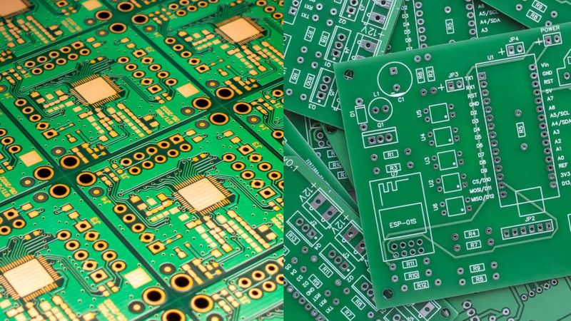
HASL vs ENIG Surface Finish
Introduction
In PCB manufacturing, surface finishes play a crucial role in protecting exposed copper traces and ensuring optimal performance. These finishes act as a barrier against oxidation and facilitate reliable soldering connections, directly impacting the functionality and longevity of electronic devices. Two prevalent surface finishes, HASL (Hot Air Solder Level) and ENIG (Electroless Nickel Immersion Gold) have emerged as popular options due to their distinct advantages and disadvantages.
The HASL process involves immersing the PCB in molten solder, followed by a hot air drying step. On the other hand, ENIG involves applying a layer of nickel followed by a thin layer of gold. Careful choice of HASL vs ENIG can significantly impact the solderability, shelf life, and overall reliability of a Printed Circuit Board (PCB).
This article will delve into a comparative analysis of HASL vs ENIG, helping you make an informed decision based on factors such as cost, solderability, and long-term performance. Still, curious about HASL vs ENIG? Let’s start with understanding the role of surface finishes in PCB manufacturing.
The Role of Surface Finishes in PCB Manufacturing
Surface finishes are protective coatings applied to the exposed copper circuitry of printed circuit boards (PCBs) after the etching process. These finishes serve as a crucial interface between the bare copper and the components that will be soldered onto the board. In PCB production, surface finishes play a multifaceted role in ensuring the quality, reliability, and longevity of the final product.
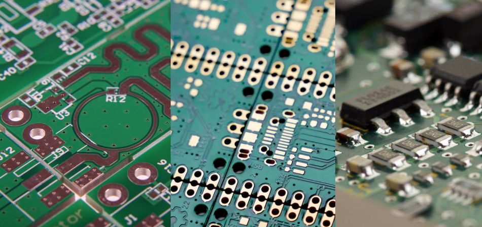
The primary purpose of surface finishes is to prevent oxidation of the exposed copper. This exposed copper can significantly degrade the solderability and electrical performance of the board over time. By creating a barrier between the copper and the environment, surface finishes maintain the integrity of the conductive pathways and connection points on the PCB.
Surface finishes have a profound impact on several key aspects of PCB performance:
Solderability: The finish directly affects how well components can be soldered to the board. A good surface finish ensures consistent and reliable solder joints, which are critical for the electrical and mechanical integrity of the assembly.
Shelf Life: Different finishes offer varying degrees of protection against oxidation and environmental factors, influencing how long a PCB can be stored before use without degradation.
Overall Performance: The choice of surface finish can impact electrical conductivity, corrosion resistance, and even the board's ability to withstand thermal cycling and harsh environments.
Selecting the appropriate surface finish is crucial and depends on various factors, including the intended application, environmental conditions, component types, and manufacturing processes. For instance, high-frequency applications may require finishes with specific electrical properties. On the other hand, boards destined for harsh environments might need finishes with superior corrosion resistance.
Key functions of surface finishes include:
Protection against oxidation and corrosion
Enhancement of solderability and solder joint reliability
Preservation of electrical conductivity
Extension of PCB shelf life
Facilitation of fine-pitch and high-density designs
Improvement of visual inspection and automated optical inspection (AOI) processes
Compatibility with various assembly technologies (e.g., reflow, wave soldering)
Contribution to the overall reliability and durability of the electronic assembly
Understanding these roles is essential for engineers and manufacturers to make informed decisions about surface finish selection. This ultimately contributes to the production of high-quality and reliable electronic devices.
HASL: Hot Air Solder Leveling
Hot Air Solder Leveling (HASL) is a widely used surface finish in PCB manufacturing, known for its cost-effectiveness and reliable soldering capabilities. The HASL process involves applying a thin, even coating of solder to the copper pads and traces of a PCB. This technique provides protection against oxidation and enhances solderability.
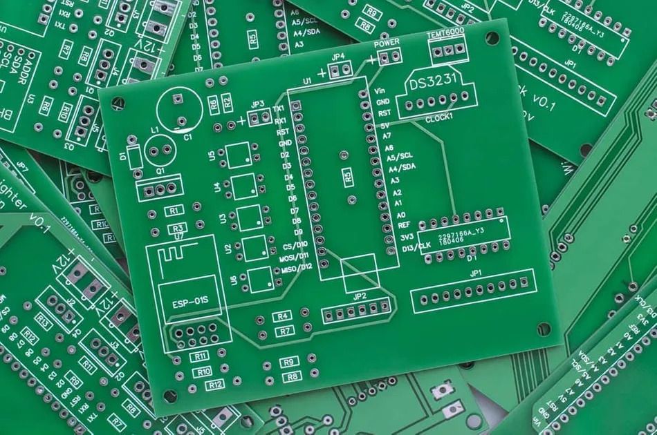
The HASL process begins with a thorough cleaning of the PCB to remove any contaminants, residues, oils, or oxides that could interfere with solder adhesion. Once cleaned, the board is submerged in a molten solder bath. The composition of this bath varies depending on whether a leaded or lead-free HASL is being applied.
Leaded HASL typically uses a combination of tin and lead, while lead-free HASL employs alternatives such as tin and silver or tin and copper. [1] The choice between leaded and lead-free options is often driven by environmental regulations and application requirements.
After the solder bath, the PCB undergoes the critical hot air levelling step. Hot air knives blow across the surface of the board, removing excess solder and creating a smooth, even layer on the pads. This step is crucial for ensuring uniform thickness and preventing issues with component placement during assembly.
The technical details of the HASL application process are as follows:
Cleaning: The PCB is cleaned using chemical or mechanical methods to ensure a contaminant-free surface.
Flux Application: A thin layer of flux is applied to improve solder wetting.
Preheating: The board is preheated to minimize thermal shock.
Solder Immersion: The PCB is dipped into the molten solder bath (typically at 230-260°C for leaded solder, or 250-280°C for lead-free).
Hot Air Leveling: Precisely controlled hot air knives (at temperatures around 400-450°C) blow away excess solder.
Cooling: The board is cooled to room temperature, allowing the solder to solidify.
Post-Treatment: Any excess flux is removed, and the board is inspected for quality.
The resulting HASL finish provides excellent protection against oxidation while maintaining high solderability for components. However, it's worth noting that HASL may be less suitable for fine-pitch components due to the potential variability in solder thickness.
To better understand the differences between leaded and lead-free HASL, consider the following comparison table:
| Property | Leaded HASL | Lead-Free HASL |
| Composition | Tin-Lead | Tin and Silver/Tin and Copper |
| Cost | Lower | Higher |
| Environmental Impact | Less Favorable (Toxic) | More Favorable (Eco-Friendly) |
| Solderability | Good | Excellent |
| Durability | Moderate | Better |
This comparison highlights the trade-offs between leaded and lead-free HASL options, with lead-free alternatives offering improved environmental compatibility and performance characteristics at a higher cost.
Advantages of HASL
Hot Air Solder Leveling (HASL) remains a popular choice for PCB surface finish due to its numerous advantages. This time-tested method offers a combination of cost-effectiveness, reliability, and ease of use that makes it attractive for a wide range of applications.
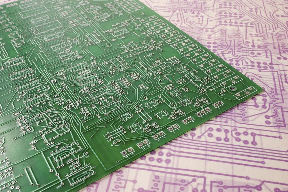
The primary benefits of HASL stem from its robust nature and compatibility with traditional soldering processes. The solder coating provides excellent protection for the underlying copper, ensuring the long-term reliability of the PCB. Moreover, the inherent properties of the solder finish contribute to its widespread adoption in the electronics industry.
Key advantages of HASL include:
Cost Effectiveness: HASL is one of the most economical surface finish options available, making it ideal for high-volume production and budget-conscious projects.
Excellent Solderability: The pre-applied solder layer ensures superior wetting during the soldering process, resulting in reliable and consistent solder joints.
Long Shelf Life: HASL-finished boards can typically be stored for extended periods without significant degradation of solderability, often up to 12 months or more. [2]
Durability: The solder coating provides good protection against oxidation and environmental factors, contributing to the longevity of the PCB.
Ease of Rework: HASL finishes allow for easy rework and repair of solder joints, which can be crucial for prototyping or field repairs.
Compatibility: HASL is compatible with a wide range of soldering techniques, including wave soldering, reflow soldering, and hand soldering.
Proven Track Record: With decades of use in the industry, HASL has a well-established reputation for reliability and performance.
Visual Inspection: The reflective nature of the solder finish allows for easy visual inspection of solder joints, aiding in quality control processes.
The combination of these advantages makes HASL particularly suitable for applications where cost is a primary concern, or where robust solderability is crucial. Industries such as consumer electronics, automotive, and industrial control systems often benefit from this balance of performance and economy.
Furthermore, the availability of lead-free HASL options has addressed environmental concerns. This allows manufacturers to comply with regulations like RoHS while still leveraging the benefits of this surface finish. This adaptability has helped HASL maintain its relevance in modern PCB manufacturing processes, even as newer finish technologies have emerged.
Limitations of HASL
While Hot Air Solder Leveling (HASL) offers numerous advantages, it also comes with several limitations that can impact its suitability for certain applications. These drawbacks have become more pronounced as electronic designs have evolved towards higher densities and finer pitches.
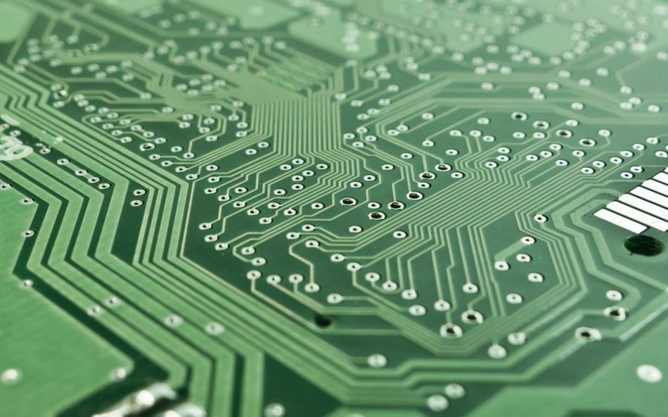
One of the primary challenges associated with HASL is its inconsistent surface planarity. The hot air leveling process can result in a non-uniform solder thickness across the board, creating a slightly domed or rounded surface on the pads. This lack of flatness can lead to issues during component placement and soldering, particularly for fine-pitch and area array packages.
Environmental concerns have also emerged as a significant consideration, especially with traditional lead-based HASL. While lead-free alternatives are available, they often come with their own set of challenges, including higher processing temperatures and potential reliability issues.
The most significant limitations of HASL, ranked in order of importance, are:
Poor Planarity: The uneven surface can cause problems with fine-pitch components and Ball Grid Array (BGA) devices, leading to potential soldering defects and reduced yield.
Fine Pitch Limitations: The relatively thick and variable coating of HASL makes it less suitable for components with pitches below 0.5mm, restricting its use in high-density designs.
Environmental Concerns: Traditional lead-based HASL poses environmental and health risks, while lead-free alternatives may have different wetting characteristics and require higher soldering temperatures.
Thickness Variability: The inconsistent solder thickness can affect the electrical performance of high-frequency circuits and impedance-controlled designs.
Aesthetic Appearance: HASL finishes can have a duller, less uniform appearance compared to other surface finishes, which may be a concern for visible PCB applications.
Shelf Life Limitations: While generally good, the shelf life of HASL is shorter than some alternative finishes, potentially impacting the long-term storage of PCBs.
Processing Temperature: HASL requires high temperatures during the application, which can cause warpage or damage to heat-sensitive PCB materials.
Limited Protection: HASL provides less protection against harsh environments compared to some other finishes, potentially affecting long-term reliability in challenging conditions.
These limitations have led many manufacturers to explore alternative surface finishes, particularly for high-performance and fine-pitch applications. However, HASL remains a viable option for many standard PCB designs where its advantages outweigh these drawbacks.
Recommended Reading: PCB Surface Finish: The Ultimate Guide to Understanding and Choosing the Right Option
ENIG: Electroless Nickel Immersion Gold
Electroless Nickel Immersion Gold (ENIG) is a sophisticated surface finish technique widely used in the printed circuit board (PCB) industry. This process involves depositing a layer of nickel followed by a thin layer of gold onto the copper pads and traces of a PCB, providing excellent solderability, corrosion resistance, and a flat surface ideal for fine-pitch components.
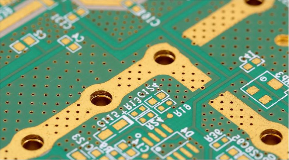
The ENIG process consists of several key steps, as illustrated in the following flowchart:
1. Cleaning: The PCB is thoroughly cleaned to remove any contaminants, oxides, or residues that could interfere with the deposition process.
2. Nickel Deposition: An electroless nickel plating process deposits a layer of nickel onto the exposed copper surfaces. [3] This layer typically ranges from 3 to 6 μm in thickness. The chemical reaction involved is:
Ni²⁺ + 2H₂PO₂⁻ + 2H₂O → Ni + 2H₂PO₃⁻ + 2H⁺ + H₂
This reaction is autocatalytic, meaning once initiated, it continues without the need for external electrical current.
3. Gold Deposition: A thin layer of gold is deposited onto the nickel surface through an immersion process. This gold layer is typically 0.05 to 0.1 μm thick. The chemical reaction for this step is:
Au⁺ + Ni → Au + Ni²⁺
This displacement reaction occurs because gold is more noble than nickel, causing nickel atoms to be replaced by gold atoms at the surface.
4. Rinse: The board is thoroughly rinsed to remove any residual chemicals and prevent contamination.
5. Drying: Finally, the PCB is dried, completing the ENIG process.
The nickel layer serves as a diffusion barrier, preventing the gold from migrating into the copper and the copper from diffusing through to the surface. It also provides a strong, corrosion-resistant foundation. The gold layer protects the nickel from oxidation and provides an excellent surface for soldering and wire bonding.
The thickness of each layer is crucial for the performance of the ENIG finish. The nickel layer must be thick enough to prevent copper diffusion but not so thick as to cause stress in the plating. The gold layer must be thin enough to be easily displaced during soldering but thick enough to prevent nickel oxidation.
The chemical process of ENIG results in a very flat surface finish, making it ideal for fine-pitch components and ball grid arrays (BGAs). The gold surface also maintains its solderability for an extended period, often exceeding 12 months. This is beneficial for components with long storage times before assembly.
Advantages of ENIG
Electroless Nickel Immersion Gold (ENIG) has gained significant popularity in the PCB industry due to its numerous advantages over other surface finishes. Its unique properties make it particularly suitable for high-performance and demanding applications in modern electronics.
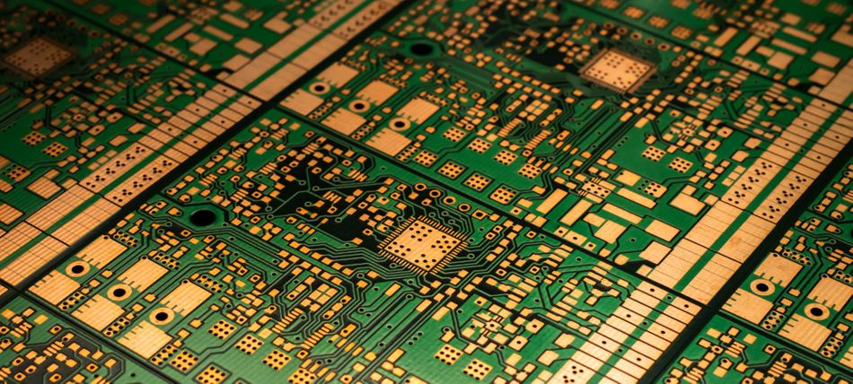
The benefits of ENIG stem from its dual-layer structure: a thick nickel layer providing durability and corrosion resistance, topped with a thin gold layer offering excellent solderability and protection. This combination results in a surface finish that addresses many challenges faced in PCBA and long-term reliability.
Key advantages of ENIG include:
Exceptional Flatness: The chemical deposition process results in a highly planar surface, crucial for fine-pitch components and ensuring consistent solder joint formation.
Fine Pitch Compatibility: The flat and uniform surface of ENIG is ideal for ultra-fine pitch devices, ball grid arrays (BGAs), and chip scale packages (CSPs), allowing for high-density designs.
Extended Shelf Life: The gold layer protects the underlying nickel from oxidation, maintaining solderability for up to 12 months or more, significantly longer than many other finishes.
Excellent Solderability: The gold surface provides consistent wetting and reliable solder joint formation across various soldering processes.
Multiple Soldering Cycles: ENIG can withstand multiple heat cycles, making it suitable for applications requiring rework or multiple assembly steps.
Wire Bonding Compatibility: The gold surface is ideal for both solder connections and wire bonding, offering versatility in assembly methods.
Uniform Thickness: The electroless process ensures consistent plating thickness across the board, including in high-aspect-ratio holes and vias.
RoHS Compliance: ENIG is a lead-free finish, meeting environmental regulations and sustainability requirements.
Corrosion Resistance: The nickel-gold combination provides excellent protection against various environmental factors, enhancing long-term reliability.
Visual Inspection: The bright, uniform gold surface facilitates easy visual inspection and automated optical inspection (AOI) processes.
The combination of flatness, fine-pitch compatibility, and extended shelf life in ENIG makes it valuable in industries where reliability and performance are top priorities. These industries include aerospace, medical devices, and high-end consumer electronics. Its ability to maintain solderability over time also reduces waste and rework in manufacturing processes with long lead times between PCB fabrication and assembly.
The superior electrical properties of ENIG and its compatibility with both traditional and advanced assembly techniques make it a preferred choice for applications in modern electronics manufacturing.
Limitations of ENIG
While Electroless Nickel Immersion Gold (ENIG) is a popular surface finish due to its excellent flatness, corrosion resistance, and long shelf life, it also has limitations. These limitations become more significant in specific manufacturing environments and advanced designs that push the boundaries of PCB technology.

One of the most critical concerns with ENIG is its susceptibility to "black pad" defects. [4] This occurs during the nickel immersion process, where excess phosphorus can cause corrosion between the nickel and gold layers, leading to poor solder joint reliability. Black pad issues can result in open circuits and severely impact the board's performance over time.
Cost is another key factor, as ENIG tends to be more expensive than other surface finishes like HASL. The multi-step deposition process, combined with the use of gold, increases production costs, making it less suitable for cost-sensitive designs.
The most significant limitations of ENIG, ranked in order of importance, are:
Black Pad Defects: This can cause solder joint failure, leading to reliability issues, particularly in mission-critical applications.
Higher Cost: ENIG is more expensive compared to HASL and other finishes due to its complex manufacturing process and the use of gold.
Brittle Solder Joints: The gold layer can sometimes cause brittle solder joints, which may be prone to cracking under mechanical stress.
Electrolytic Contamination: Poor control during the electroless nickel plating process can introduce contamination, which affects both electrical and mechanical performance.
Rework Complexity: ENIG-coated boards can be more challenging to rework, particularly for boards that require multiple reflow cycles.
Thermal Stress: ENIG may not perform as well under extreme thermal cycling, which can lead to fractures in the nickel layer, affecting long-term reliability.
Compatibility Issues: Certain components may not be fully compatible with ENIG, leading to potential challenges in assembly and long-term performance.
Limited Repairability: Once applied, ENIG's finish can be difficult to repair or reapply without affecting its properties.
While ENIG is favored for high-performance, high-density PCB designs, these limitations often prompt manufacturers to carefully weigh their options based on specific project requirements.
Recommended Reading: Understanding the ENIG Finish: A Comprehensive Guide
HASL vs ENIG: A Head-to-Head Comparison
When selecting a surface finish for printed circuit boards (PCBs), engineers and manufacturers must carefully weigh the pros and cons of each option. Hot Air Solder Leveling (HASL) and Electroless Nickel Immersion Gold (ENIG) are two popular choices, each with distinct characteristics that affect their suitability for different applications.
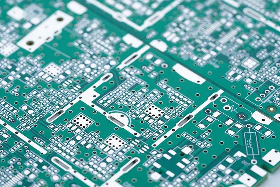
The following table provides a comprehensive comparison of HASL and ENIG across key parameters:
| Parameter | HASL | ENIG |
| Cost | Low | High |
| Durability | Good | Excellent |
| Planarity | Poor to Fair | Excellent |
| Fine Pitch Compatibility | Limited (>0.5mm Pitch) | Excellent (<0.3mm Pitch) |
| Shelf Life | 6-12 months | 12-18 months |
| Environmental Impact | Higher (Lead-Based)/ Moderate (Lead-Free) | Low |
| Thickness Consistency | Variable (1-50 µm) | Highly Consistent (3-6 µm Ni, 0.05-0.1 µm Au) |
| Solderability | Excellent | Good to Excellent |
| Wire Bonding Compatibility | Poor | Excellent |
| RoHS Compliance | Varies (Lead-Free Option Available) | Yes |
Detailed analysis of comparison points:
Cost: HASL is generally more cost-effective, with prices ranging from $0.10 to $0.30 per square inch, while ENIG typically costs between $0.30 to $0.60 per square inch. The higher cost of ENIG is due to the use of gold and the more complex process.
Durability: ENIG offers superior durability due to its nickel barrier layer, which provides excellent corrosion resistance. HASL, while durable, may be more susceptible to oxidation over time.
Planarity: The chemical deposition process in ENIG results in a highly planar surface with variations typically less than 0.1 µm. The mechanical process in HASL can lead to surface variations of 10-20 µm, which can be problematic for fine-pitch components.
Fine-pitch Compatibility: The excellent planarity in ENIG makes it suitable for components with pitches below 0.3mm, adhering to IPC-7351B standards for ultra-fine pitch devices. HASL is generally limited to components with pitches above 0.5mm due to its uneven surface.
Shelf Life: The gold layer in ENIG provides superior protection against oxidation, resulting in a longer shelf life of 12-18 months. HASL typically offers a shelf life of 6-12 months before solderability degradation becomes a concern.
Environmental Impact: Lead-free HASL and ENIG are both environmentally friendly options. However, traditional lead-based HASL poses environmental concerns and is restricted in many regions due to RoHS regulations.
Thickness Consistency: ENIG provides highly consistent plating thickness, crucial for impedance-controlled circuits and RF applications. HASL thickness can vary significantly, potentially affecting electrical performance in sensitive designs.
Solderability: Both finishes offer excellent solderability, but HASL may have a slight edge due to its pre-tinned surface. ENIG requires proper flux activation to displace the gold layer during soldering.
Rework Ability: HASL excels in rework scenarios due to its thick lead solder layer. ENIG, while suitable for rework, may require more careful temperature control to avoid damaging the thin gold layer.
Wire Bonding Compatibility: The gold surface in ENIG is ideal for wire bonding applications, meeting MIL-STD-883 pull strength requirements. HASL is generally not suitable for wire bonding due to its uneven surface and solder composition.
RoHS Compliance: All ENIG processes are inherently RoHS compliant. HASL is available in both leaded (non-RoHS) and lead-free (RoHS-compliant) versions, with the latter becoming increasingly common to meet global environmental regulations.
The choice between HASL and ENIG ultimately depends on the specific requirements of the PCB application, balancing factors such as cost, performance needs, and environmental considerations. High-reliability and fine-pitch applications often favour ENIG, while cost-sensitive projects with less demanding specifications may opt for HASL.
Recommended Reading: PCB Manufacturing Process: A Comprehensive Guide to Understanding and Mastering the Techniques
Choosing Between HASL and ENIG: Application-Specific Considerations
The selection between HASL and ENIG as a PCB surface finish depends on various factors specific to the application, design requirements, and manufacturing constraints. Understanding these considerations is crucial for making an informed decision that balances performance, cost, and reliability.
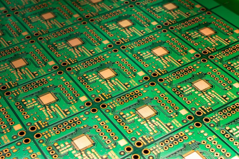
HASL is often the preferred choice in scenarios where:
Cost is a primary concern, especially for high-volume production
The PCB design features relatively large pad sizes and pitch (>0.5mm)
Excellent solderability is required for through-hole SMD/SMT components
The product has a shorter expected lifespan or operates in less demanding environments
Quick turnaround time is essential, as HASL is typically faster to apply
ENIG becomes more suitable in situations where:
The PCB design incorporates fine-pitch components (<0.5mm) or BGAs
Flatness is critical for assembly, especially with automated pick-and-place equipment
Extended shelf life is required, often exceeding 12 months
The application involves both soldering and wire bonding
Environmental regulations demand lead-free finishes
The product operates in harsh or corrosive environments
Industry examples for each surface finish are below:
HASL is commonly used in:
Consumer Electronics (e.g., Household Appliances, Toys)
Automotive Non-Critical systems (e.g., Infotainment Systems)
Industrial Control Equipment
Power Supplies and LED lighting
ENIG is typically preferred in:
Aerospace and Defense Electronics
Medical Devices
High-Frequency RF Applications
Telecommunications Equipment
High-End Consumer Electronics (e.g., Smartphones, Tablets)
Some of the other commonly used types of surface finishes in printed circuit board manufacturing are as follows:
OSP (Organic Solderability Preservatives): This process involves applying a thin layer of an organic compound to the printed circuit board surface to protect it from oxidation and improve its solderability.
Immersion Tin: In this, the surface finish involves coating the printed circuit board with a layer of tin, which provides good corrosion resistance and low contact resistance.
ENEPIG (Electroless Nickel Electroless Palladium Immersion Gold): In this, the surface finish is an advanced version of ENIG with improved corrosion resistance and excellent shelf life.
Immersion Silver: The surface finish involves the coating of the printed circuit board with a layer of silver, similar to Immersion Tin, and provides good corrosion resistance.
Gold Plating: As the name suggests, the surface finish involves the coating of the printed circuit board with a layer of gold.
Consulting with PCB manufacturers and considering the entire product lifecycle can help in making the optimal choice between HASL and ENIG for a given application.
Conclusion
The choice between HASL and ENIG surface finishes significantly impacts PCB performance, reliability, and manufacturing processes. HASL offers cost-effectiveness and excellent solderability, making it suitable for many standard applications. In contrast, ENIG provides superior planarity, fine-pitch compatibility, and extended shelf life, ideal for high-performance and demanding environments. When selecting a surface finish, consider factors such as component density, environmental conditions, expected product lifespan, and budget constraints. Ultimately, the decision should align with specific project requirements, balancing technical needs against economic considerations. Consulting with PCBA manufacturers and conducting thorough testing can help ensure the optimal surface finish choice for your application.
Frequently Asked Questions
Q: Can HASL be used for fine-pitch components?
A: While HASL can be used for components with pitches down to about 0.5mm, it's generally not recommended for finer pitches due to its uneven surface. For ultra-fine pitch components (<0.5mm), ENIG is typically the better choice.
Q: Is ENIG always more expensive than HASL?
A: Yes, ENIG is generally more expensive than HASL due to the use of hard gold and the more complex manufacturing process. However, the cost difference may be offset by improved yield and reliability in certain applications.
Q: How does the thickness of HASL and ENIG compare?
A: HASL thickness can vary significantly, typically ranging from 1 to 50 μm. ENIG provides a more consistent finish, with a nickel layer of 3-6 μm and a gold layer of 0.05-0.1 μm.
Q: Are there any reliability concerns specific to ENIG?
A: One potential issue with ENIG is "black pad syndrome," where a corrosion layer forms between the nickel and gold, leading to poor solder joint reliability. However, modern ENIG processes have largely mitigated this issue.
Q: How does the choice between HASL and ENIG affect PCB assembly processes?
A: ENIG's flat surface facilitates more accurate component placement and is compatible with both reflow and wave soldering. HASL may require more precise control during assembly due to its uneven surface but generally offers excellent solderability.
References
[1] RAY PCB. What’s the Difference Between HASL and HASL Lead-Free in PCB? [Cited 2024 September 25] Available at: Link
[2] Venture MFG. PCB Surface Finish Types [Cited 2024 September 25] Available at: Link
[3] Nickel Institute. Properties and Applications of Electroless Nickel [Cited 2024 September 25] Available at: Link
[4] Hileap Electronic. Understand what is ENIG Black Pad, and How to Avoid? [Cited 2024 September 25] Available at: Link
Table of Contents
IntroductionThe Role of Surface Finishes in PCB ManufacturingHASL: Hot Air Solder LevelingAdvantages of HASLLimitations of HASLENIG: Electroless Nickel Immersion GoldAdvantages of ENIGLimitations of ENIGHASL vs ENIG: A Head-to-Head ComparisonChoosing Between HASL and ENIG: Application-Specific ConsiderationsConclusionFrequently Asked QuestionsReferences