How to Make a PCB: Theoretical Concepts and Practical Implementation
A step-by-step guide on designing and fabricating modern printed circuit boards (PCBs) for professional and academic applications.

31 Mar, 2025. 17 minutes read
No time now? Save for later.
We only use your email to send this link. Privacy Policy.
Key Takeaways:
Understand PCB design fundamentals, including schematic capture, layout, component placement, and signal integrity considerations.
Overview of modern PCB manufacturing techniques, from CNC prototyping to industrial fabrication processes.
Key considerations in PCB material selection (FR-4 vs advanced substrates), design rules, and fabrication constraints.
Testing and quality assurance are important in PCB production, including electrical tests, AOI, and functional testing.
Emerging trends in PCB technology, such as HDI (high-density interconnect), flexible PCBs, and additive manufacturing of electronics.
Introduction
The increasing complexity of electronic devices demands high-quality PCB design and manufacturing. From smartphones to aerospace systems, printed circuit boards form the backbone of virtually all modern electronics. Over the decades, PCB technology has evolved significantly – moving from simple single-sided boards to multi-layer high-density interconnects – to keep up with the drive for smaller, faster, and more reliable devices. This evolution in PCB technology has enabled mass production of complex circuits with excellent repeatability and lower costs, replacing old wiring methods like point-to-point wiring and wire wrapping.
This guide explains the entire process of designing and fabricating a PCB using modern methods. It will cover the theoretical concepts of PCB and its types. of PCBs, a step-by-step PCB design process, preparing design files for fabrication (like Gerber files), and how to choose a PCB manufacturer. The article also delves into PCB manufacturing techniques, comparing DIY approaches (such as CNC milling) with professional fabrication, and discusses assembly methods (surface-mount vs. through-hole). Moreover, it will address testing and quality assurance for finished boards, and explore future trends in PCB manufacturing including HDI technology, flexible circuits, and additive manufacturing of electronics.
What is a PCB?
A printed circuit board (PCB) is a laminated board that mechanically supports and electrically connects electronic components using conductive copper traces, pads, and other features etched from copper sheets laminated onto a non-conductive substrate.
Components like microchips, resistors, and connectors are soldered onto the PCB’s surface (or inserted through holes) to create a complete, functional assembly. PCBs not only provide physical support to components but also ensure reliable electrical connections between them.
Suggested Reading: PCB Components: A Comprehensive Technical Guide to Passive, Active, and Electromechanical Parts

Types of PCBs
Printed circuit boards come in several types and configurations, each suited to different applications:
Single-Layer PCB (Single-Sided): This is the simplest type of PCB, with copper traces on only one side of the substrate. All components and circuits are on that single copper layer. Single-layer PCBs are easy to design and manufacture, making them low-cost. They are commonly used in basic, low-density circuits such as simple gadgets, calculators, or power supplies, but they have a limited wiring capacity because of just one side available for routing.
Double-Layer PCB (Double-Sided): These PCBs have copper layers on both sides of the substrate. Holes drilled through the board (vias) allow connections between the top and bottom copper layers. This effectively doubles the routing area and can accommodate more complex circuits than single-sided boards. Double-layer PCBs allow components to be spread on both sides and use either through-hole or surface-mount components.
Multi-Layer PCB: These PCBs have three or more copper layers, stacked with insulating layers in between and interconnected by vias. For example, a 4-layer PCB might have two inner copper layers for power and ground planes, in addition to top and bottom layers for signals. Multilayer boards greatly increase wiring density and circuit complexity. They are mainly used to route high-pin-count chips and high-density circuits in a compact area. Common applications include computer motherboards, smartphones, and other advanced electronics.
Suggested Reading: PCB Layers: Everything You Need to Know
Rigid PCB: A rigid PCB uses a solid, inflexible substrate (typically FR-4 fiberglass epoxy). Once manufactured, it retains a fixed shape. Rigid PCBs are by far the most common type – for example, the motherboard in a PC or the controller board in a TV are rigid PCBs. They can be single-layer or multi-layer. Rigid boards provide mechanical stability and are easier to assemble in products that require the board to hold its shape permanently.
Flexible PCB (Flex Circuit): In contrast to rigid boards, flexible PCBs are built on flexible plastic substrates (like polyimide Kapton) that can bend and flex without breaking the circuits. Flex circuits can be single, double, or multi-layer as well, but use thin, bendable materials. These boards are useful in tightly packed or dynamic environments – for example, inside foldable devices, cameras, or wearable electronics – where the PCB needs to conform to a shape or tolerate motion. Flexible PCBs tend to cost more to fabricate due to specialized materials, but they enable designs that are lightweight and can fold or twist, replacing the need for connectors and cables in some cases.
Suggested Reading: Rigid Flex PCB: Revolutionizing Modern Electronics Design
Step-by-Step PCB Design Process
Designing a PCB is a multi-step process that transforms an electrical schematic into a physical board ready for fabrication. It requires careful planning and adherence to both electrical and manufacturing guidelines. Below is a step-by-step breakdown of the PCB design process:
Circuit Design and Schematic Capture
Every PCB project begins with a circuit design, which involves defining the electronic components needed and how they connect to each other. This is typically done by creating a schematic diagram using electronic design automation (EDA) software.
Schematic capture is the process of designing the blueprint of the circuit. At this stage, the physical layout of the circuit is not realized. The process involves the following steps:
Drawing the circuit diagram in the software
Placing symbols for each component (resistors, capacitors, ICs, connectors, etc.)
Drawing nets (wires) to connect pins according to the circuit’s logic.
In this phase, the designer chooses specific component values and reference designators (e.g., R1 for a resistor, U1 for an IC) and ensures the circuit meets the desired functional requirements. It’s crucial to double-check that the schematic is correct because any mistake here will propagate to the PCB. Many EDA tools provide electrical rule checks to catch errors like unconnected pins or short circuits in the schematic.
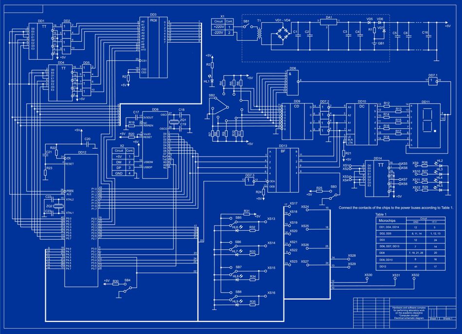
Once the schematic is complete, the EDA tool can generate a netlist – a list of all the connections – and associate each schematic component with a physical footprint (the land pattern that will be used on the PCB for that component).
PCB Layout, Component Placement, Routing, and DRC
PCB layout design is where the schematic turns into an actual board design. This involves deciding the board outline, placing components, and routing copper traces to connect the components according to the schematic netlist. ]The designer’s job is to place components in sensible locations and draw the copper traces (or use an auto-router for parts of the job) while following a host of design rules and best practices.
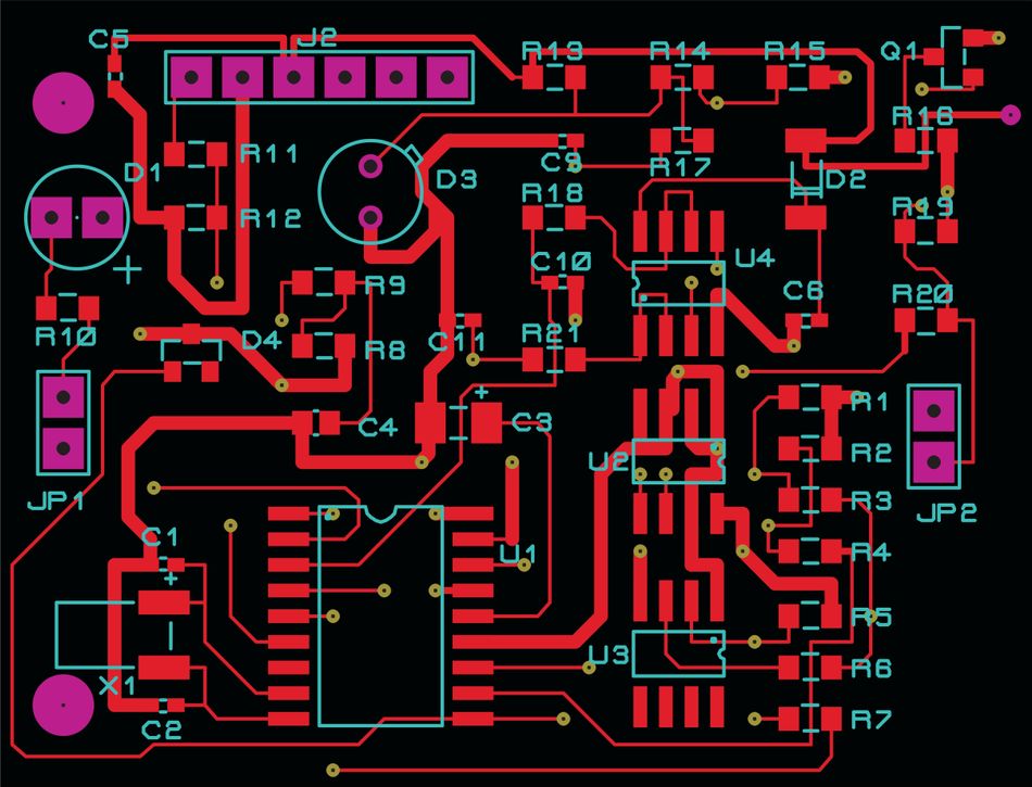
Component placement is a critical first task. Parts should be positioned to optimize electrical performance and manufacturability. For instance, you might cluster related components (like decoupling capacitors right next to the IC they serve) to shorten connections and reduce noise. You also need to consider physical constraints: connector locations, mechanical mounting holes, and keep-out areas. A good placement optimizes for short, direct routing of high-speed signals and clear separation between different functional blocks (like keeping analog sections away from noisy digital sections).
Next comes routing the PCB traces. Each connection (net) from the schematic must be implemented as a copper trace on one of the board’s layers. The designer chooses trace widths based on current requirements (wider traces for higher current carrying) and space constraints. They also determine via placements to jump between layers if it’s a multi-layer board. All routing must obey design rules – these are constraints like minimum trace width, minimum spacing between traces, minimum annular ring around via holes, etc., which are typically dictated by the PCB manufacturer’s capabilities.
Throughout the layout process, it’s important to run periodic Design Rule Checks (DRC). DRC is an automated check that scans the layout to ensure that all rules are being followed and that there are no clearances issues, unconnected nets, or other layout errors. This helps catch mistakes early, such as traces that are too close together or a missing connection that was overlooked.
Signal Integrity, Power, and Thermal Considerations
While placing components and routing traces, engineers must pay special attention to signal integrity (SI), power distribution, and thermal management – especially in high-speed or high-power designs. These considerations ensure that the PCB will perform reliably in the intended application without electrical noise or overheating issues.
Signal Integrity: High-frequency or fast edge-rate signals can suffer degradation (like reflections, crosstalk, and electromagnetic interference) if the PCB layout isn’t optimized. To maintain signal integrity, designers use techniques such as controlled impedance traces for high-speed lines, proper termination of transmission lines, and keeping critical signals (e.g., clock lines) short and direct.
Trace geometry Avoiding 90-degree sharp trace bends is a common rule since right-angle corners can cause impedance change and signal reflection. Instead, traces are routed with gentle curves or 45° angles. High-speed signals should be routed away from sensitive analog traces to prevent coupling, and if running on parallel adjacent layers, they are routed at perpendicular angles to each other to minimize crosstalk.
Power Distribution and Grounding: A stable power delivery network on the PCB is crucial. This typically involves using power planes and ground planes (solid copper areas) for distributing power to components. A multilayer PCB often dedicates one or more entire layers to be a ground plane and a power plane. When multiple supply voltages are present, each may use separate zones or planes, or sometimes share planes if carefully partitioned. Designers also sprinkle decoupling capacitors near IC power pins, connecting them between power and ground. These capacitors locally stabilize the supply voltage by providing bursts of current to the ICs during fast switching events, thereby maintaining power integrity.
Thermal Considerations: Some components or boards carrying significant currents can generate heat. PCBs must be designed to dissipate this heat to avoid hotspots that could damage components or affect performance.
One approach is to use thermal vias – arrays of vias under a hot component (like a power regulator or LED) that help conduct heat to other layers or to a copper plane that can spread or sink the heat.
Another is to leave sufficient copper area (sometimes called copper pours or heatsink pads) around high-power components to radiate heat. In high-density or high-power boards, the PCB material selection can also play a role: for instance, using substrates with higher glass transition temperature (Tg) or metal-core PCBs for LED lighting where heat dissipation is critical.
Material Selection and High-Speed Considerations: The standard PCB substrate, FR-4, is suitable for the vast majority of designs. However, for very high frequency circuits (RF/microwave or high-speed digital beyond a few GHz), FR-4’s dielectric properties may introduce too much signal loss or skew. In such cases, special low-loss laminate materials (like Rogers or Teflon-based laminates) are used which have more stable dielectric constants at high frequencies. These materials help maintain signal integrity for high-speed signals but are more expensive.
Suggested Reading: PCB Layout: A Comprehensive Guide
Preparing for Fabrication
Once the PCB layout is complete and thoroughly checked, the next phase is preparing everything needed to have the board manufactured. PCB fabrication is typically done by specialized PCB manufacturers (also called fab houses). Here are the key steps in preparing for fabrication:
Generate Manufacturing Files
PCB manufacturers require specific files that describe each layer of the PCB design. The most common format is the Gerber file (RS-274X standard). Gerber files are 2D ASCII vector files that precisely describe the copper traces, solder masks, silkscreen markings, and other board features for each layer of the PCB.
A typical PCB design will output a set of Gerbers: one file per copper layer, plus files for the solder mask layers, silkscreen layers, and sometimes other instructions (like a mechanical drawing layer).
After generating Gerbers, it’s good practice to inspect them with a Gerber viewer to ensure everything looks correct (footprints are correct, nothing missing, layers align, etc.). T Many PCB CAD tools can also export a consolidated archive (like a ZIP) containing all the Gerbers and drill files at once. Gerbers have become the de facto standard for PCB manufacturing – they provide the exact graphical description of the PCB layers that fab machines need .
Suggested Reading: What are Gerber Files? Understanding the Blueprint of Electronics Manufacturing
Design Documentation and CAD/CAM Outputs
Other than Gerber files, there may be other output files necessary to aid the fabrication process.
For example, a Bill of Materials (BOM) listing the components (if you are also assembling the board with the manufacturer), an assembly drawing showing component placements and orientations, and a readme or fab notes specifying details like board thickness, material, solder mask color, surface finish, etc.
Some designs may also include a pick-and-place file (also called a centroid file or XY file) that has the coordinates of all components for automated assembly. If your board has multiple designs repeated (panelization), you may need to specify how you want the boards arrayed on a panel.
Choosing a PCB Manufacturer
PCB manufacturers vary in capabilities, impacting design feasibility. Consider factors like layer count, trace/hole size, materials, certifications (ISO 9001, IPC class qualifications, UL certifications), cost, and assembly services. For simple boards, most services suffice; complex HDI designs require specialized manufacturers. Review design rules to ensure your layout matches their process limits.
Choose between prototyping and production services based on your needs. Prototyping offers low cost and quick turnaround for small quantities, while production prioritizes volume and quality with potentially higher setup costs.
Submitting the Design for Fabrication
These days, most PCB manufacturers have an online portal where you upload your Gerber files (usually in a ZIP archive) and enter board specifications. Alternatively, you might email the files with instructions. When submitting, you will specify parameters such as: the board dimensions, number of layers, quantity of boards, thickness of the board (common default is 1.6 mm for FR-4), copper weight (e.g., 1 oz copper is standard; heavier copper for high current designs if needed), solder mask color, silkscreen color, surface finish (like HASL, ENIG, etc.), and any other options (plated vs non-plated holes, via tenting requirements, etc.).
Modern PCB Manufacturing Techniques
PCB manufacturing has come a long way from its early days. Modern techniques allow for high precision and automation, but engineers also have options for quick in-house prototyping. CNC Machining vs. Industrial PCB Fabrication
If you’re making a PCB, you generally have two paths: hand it off to a professional fabrication house (which uses industrial processes like photolithography, plating, and etching), or attempt to make the PCB yourself using a milling machine or other prototyping method (like CNC routing or even chemical etching in-house). Each approach has its uses, pros, and cons.
CNC PCB Prototyping:
A CNC milling machine can be used to fabricate PCBs by carving away copper from a copper-clad board to leave only the desired traces. Essentially, the CNC router acts like an “etching” tool mechanically. The advantage of using a CNC to make your own PCB is speed and iteration: you can design a circuit in the morning and have a board milled, drilled, and ready for testing by the afternoon, without waiting on shipping.
Limitation: Milling fine traces requires a very precise machine and bits; small features may not be achievable on a low-end CNC. It often involves a lot of manual setup and oversight – leveling the board, choosing the correct tooling, and babysitting the job to ensure the milling is done correctly. This can be labor-intensive and time-consuming, offsetting some benefits. Additionally, homemade CNC boards typically lack plated through-holes (vias) because hobby CNC machines cannot electroplate vias easily. This means vias on a CNC-made double-sided board have to be manually soldered with wires, and multi-layer boards are virtually impossible to do at home. There’s also usually no solder mask or silkscreen on DIY boards unless one goes through extra steps.
Industrial PCB Fabrication
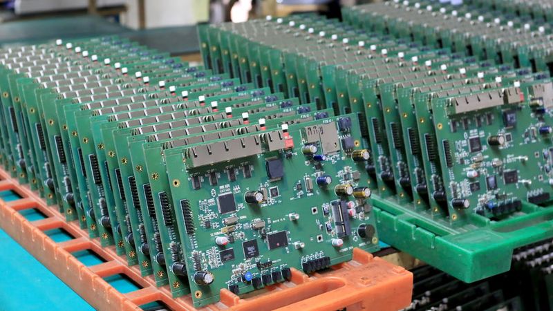
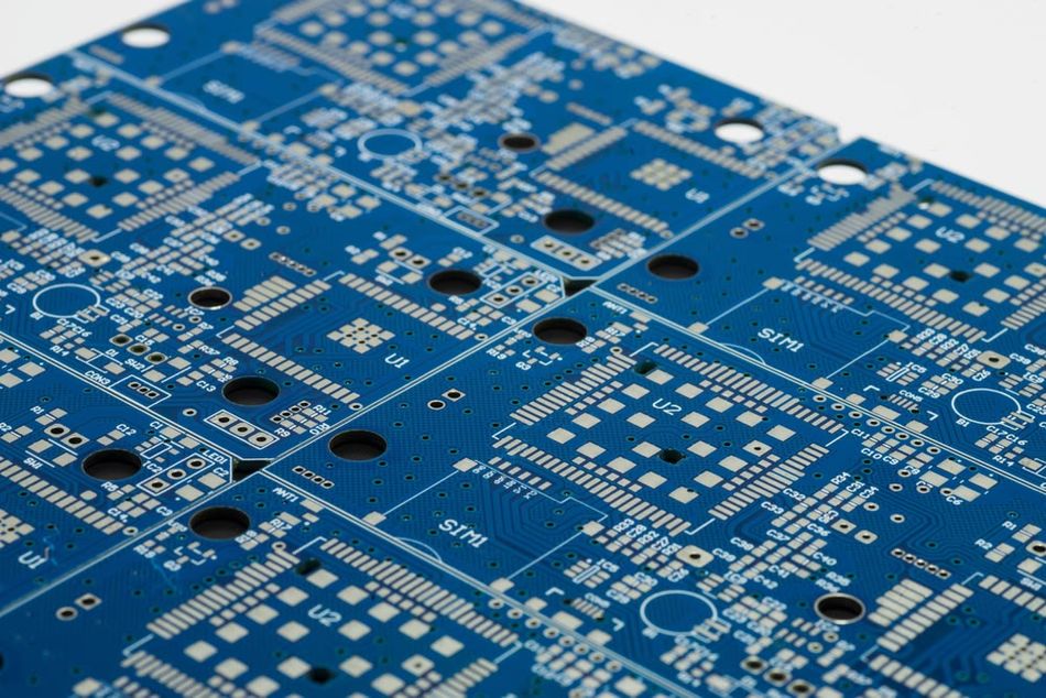
Professional PCB manufacturing is a highly automated and precise process. It typically starts with the manufacturer using your Gerber files to photo-plot the circuit patterns onto the copper-clad layers using UV light and photoresist. The unwanted copper is then chemically etched away, leaving the desired traces. For multi-layer PCBs, layers are fabricated, then laminated together under heat and pressure with insulating prepreg between them. Drilling machines (guided by the drill file) create the holes, and through-hole vias are plated with copper to form electrical connections between layers. The boards then get solder masks applied (usually by silkscreen or spray and then UV cure), and silkscreen printing for component labels. Finally, a surface finish like HASL (solder coating) or ENIG (gold over nickel) is applied to exposed copper pads to protect them and ensure solderability.
Suggested Reading: PCB Drilling: Precision Techniques for Modern Electronics
The advantage of industrial fabrication is you get high-quality boards that can be very complex. Multi-layer designs, fine line widths (on the order of a few mils), micro vias, and intricate soldermask dams are all possible with the right fabrication process. The equipment used (laser direct imaging, CNC drilling, automated plating lines, etc.) can achieve precision that is impossible with desktop milling. Also, the boards come finished with a solder mask, silkscreen, and plated holes – just like a professional product. This means you can assemble them reliably, even using tiny SMD components and BGAs.
Of course, the trade-off here is time and some upfront cost. Even rush orders from a fab usually take a day or two at minimum (plus shipping).
Surface-Mount vs. Through-Hole Assembly
After the PCB itself is fabricated (the bare board), the next step is PCB assembly – actually soldering components onto the board to build the functional circuit. There are two fundamental technologies for mounting components: Through-Hole Technology (THT) and Surface-Mount Technology (SMT). Most modern electronics primarily use SMT for components, with through-hole reserved for specific use cases.
Through-Hole Technology
Through-hole technology (THT) involves inserting component leads through drilled PCB holes and soldering them on the opposite side, creating strong mechanical bonds ideal for robust connections and large components. While THT allows for easier manual soldering and is suitable for hobbyists and initial prototyping, it increases manufacturing complexity due to drilling and limits PCB compactness due to larger component sizes.
Surface Mount Technology
Surface-Mount Technology (SMT) solders components directly onto PCB surface pads, eliminating the need for drilled holes. Solder paste is stenciled, automated pick-and-place machines position components, and a reflow oven melts the paste, bonding components to the PCB. This process results in surface-mounted components secured at their connection points.
Feature | Through-Hole Technology (THT) | Surface-Mount Technology (SMT) |
Component Mounting | Leads are inserted through drilled holes, and soldered on the opposite side. | Components are soldered directly onto surface pads. |
Mechanical Strength | Very strong mechanical bonds. | Less robust mechanically, but generally sufficient. |
Component Size | Larger packages and lead spacing (e.g., DIP ICs). | Smaller components (e.g., 0402 resistors, SOICs, QFPs). |
PCB Density | Lower component density due to larger components and hole requirements. | Higher component density, allowing smaller PCBs. |
Manufacturing Complexity | Higher due to drilling holes. | Lower drilling requirements, simpler for complex designs. |
Automation | Less suitable for high automation. | Highly automated placement and reflow process. |
Production Throughput | Lower throughput. | Higher throughput, faster assembly. |
Assembly Process | Wave soldering, and manual soldering are possible. | Solder paste application, automated pick-and-place, reflow soldering. |
Two-Sided Assembly | Difficult to solder both sides in one go. | Easily mount components on both sides. |
Component Availability | Limited availability for modern ICs. | Dominant technology for modern ICs. |
Cost | Higher cost for complex designs due to drilling. | Lower cost for complex designs due to reduced drilling and automation. |
Applications | Robust connections, large components, hobby electronics, prototyping. | High-density circuits, mass production, modern electronics. |
Manual Assembly | relatively easy to hand solder. | More difficult to hand solder. |
Suggested Reading: SMT Assembly vs. Through-Hole: What to Know
Testing and Quality Control
Designing and manufacturing a PCB is only part of the process – ensuring that the finished boards work correctly and meet quality standards is equally important. Here are key methods and considerations:
Bare Board Electrical Testing
Professional PCB fabricators electrically test each board for opens and shorts, using flying probes for low-to-mid volumes and bed-of-nails fixtures for high-volume production. These tests verify Gerber design accuracy, ensuring no trace breaks or unintended connections. Failed boards are marked or reworked, guaranteeing subsequent issues aren't due to fabrication errors.
Assembly Inspection
Once components are soldered onto the board (whether by you or a contract manufacturer), inspection is crucial to ensure assembly quality. The two main automated inspection methods are AOI (Automated Optical Inspection) and AXI (Automated X-ray Inspection).
AOI uses high-resolution cameras and image processing to scan the board for any visual defects. It can detect problems like missing components, misaligned parts, incorrect components (e.g., wrong orientation of an IC or a diode), and solder joint issues such as solder bridges (shorts between pins) or insufficient solder.
X-Ray Inspection can reveal hidden solder joint issues – for example, in a BGA it can show if any solder balls are missing or have voids, or if there are shorts under an IC that optical methods can’t see. X-ray inspection is typically used for boards with complex packages or very fine pitch where optical might miss defects. It is a bit more costly and slower than AOI, so it might be used selectively on critical boards or sample batches.
Functional Testing and Debugging
Passing optical or electrical tests doesn’t guarantee the board actually works as intended in the circuit. Functional testing involves powering up the assembled PCB and verifying it performs according to the design specifications. This could be as simple as plugging the board into a test jig that runs a predefined sequence of operations (checking voltages, making sure the microcontroller can be programmed, exercising inputs/outputs, etc.).
In an engineering context, the design team will often do this manually for prototypes: they’ll apply power carefully (perhaps with a current-limited supply to catch any shorts), verify that no component overheats, then check if all the subsystems function (clocks are oscillating, communication interfaces send data, etc.). They might use instruments like oscilloscopes, multimeters, logic analyzers, or in-circuit debuggers to verify and debug the circuit.
Conclusion
This article comprehensively covers PCB design and fabrication, emphasizing the blend of creative design and precise manufacturing. It details the process from PCB type selection and design best practices, including schematic capture and layout, to fabrication outputs and manufacturer collaboration. Modern techniques like SMT and THT are explained, along with the crucial role of testing and quality control. The article also highlights evolving PCB technologies, such as HDI and additive manufacturing, and encourages engineers to stay informed. It concludes by stressing the importance of thorough planning, design rule adherence, and verification for successful PCB creation.
FAQ
What is the difference between single-layer and multi-layer PCBs?
Single-layer PCBs offer simple, cost-effective routing on one side, suitable for low-density circuits. Multi-layer PCBs, with stacked copper layers, enable complex, high-density designs for advanced electronics, using internal layers for power/ground and external for signals. While multi-layer boards are more expensive and harder to repair, they are essential for compact, complex devices.
What are the key design rules for PCB layout?
PCB design rules ensure manufacturability and reliability. Key rules include maintaining minimum trace width and spacing, avoiding sharp bends, and using appropriate via sizes. For high-speed designs, control impedance and route differential pairs correctly. Place decoupling capacitors near IC power pins and adhere to creepage and clearance rules for high voltage. Always run a DRC before finishing to catch violations. Following these guidelines minimizes defects and performance issues.
How do I choose the right PCB manufacturer?
Selecting a PCB manufacturer requires matching design needs with manufacturer capabilities. Consider technical requirements like layer count, trace width, and materials, ensuring the manufacturer meets these specs. Evaluate quality certifications and reputation through reviews. Factor in lead time, location, and cost, choosing affordable services for prototypes and reputable fabs for critical projects. Assembly services and free DFM checks are beneficial. Match the fab to design complexity and quality needs, utilizing support for advanced boards and responsive communication.
What is the role of Gerber files in PCB fabrication?
Gerber files are essential digital blueprints that communicate PCB layout to manufacturers, with each file representing a specific layer. They guide fabrication machines in creating photomasks or directly imaging patterns. Along with drill files, Gerbers are the primary way designers instruct manufacturers. While alternatives exist, Gerber remains the industry standard, ensuring accurate reproduction of the designed PCB layers.
What are the most common PCB manufacturing defects and how to avoid them?
PCB defects include opens, shorts, misregistration, delamination, and soldering issues. DFM compliance, clean Gerbers, and reputable manufacturers reduce these. Teardrops prevent opens, suitable materials and baking prevent delamination. Proper footprint and stencil designs, plus reflow profiles and inspections, mitigate assembly defects. Design reviews and test structures also help. Quality-focused manufacturers and assembly houses, alongside meticulous design, minimize defects.
How does CNC PCB manufacturing compare to traditional etching methods?
CNC PCB milling mechanically carves copper, ideal for rapid prototyping without masks or chemicals, but limited in precision and unable to plate vias or add solder mask. Chemical etching, used in mass production, etches entire panels, achieving finer details and multilayer boards with plated vias and solder mask. CNC is quick for simple prototypes, while chemical etching via a fab offers professional-grade boards for complex designs and volume production. Hobbyists often begin with CNC for learning, transitioning to professional fabs as designs advance, especially with reduced costs and turnaround times for professional PCBs.
What are the latest advancements in PCB manufacturing technology?
PCB advancements include HDI with any-layer vias, embedded components, and improved high-frequency/thermal materials. Laser direct imaging enables finer traces, and additive manufacturing allows 3D-printed PCBs for rapid prototyping. Flexible, stretchable PCBs and AI-driven automation enhance adaptability and quality. Integrated CAD tools streamline design-to-fabrication. These innovations enable denser, more adaptable PCBs, facilitating high-speed circuits and 3D-printed designs, and broadening engineering possibilities.
References
in this article
1. Key Takeaways:2. Introduction3. What is a PCB?4. Step-by-Step PCB Design Process5. Preparing for Fabrication6. Modern PCB Manufacturing Techniques7. Testing and Quality Control8. Conclusion9. FAQ10. ReferencesNo time now? Save for later.
We only use your email to send this link. Privacy Policy.