MEMS Sensors: Miniature Marvels Revolutionizing Modern Technology
This article delves deeper into the microscopic world of MEMS sensors, exploring their operating principles, diverse applications, and the cutting-edge advancements propelling them into the future.

15 Jul, 2024. 14 minutes read
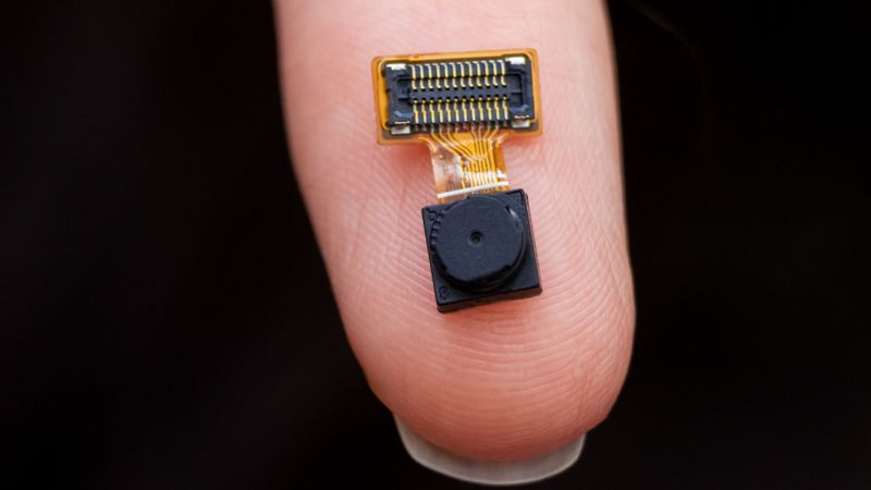
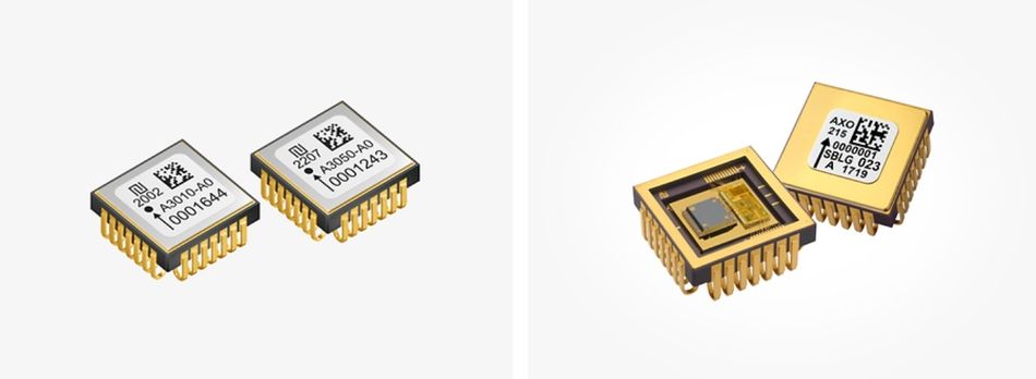
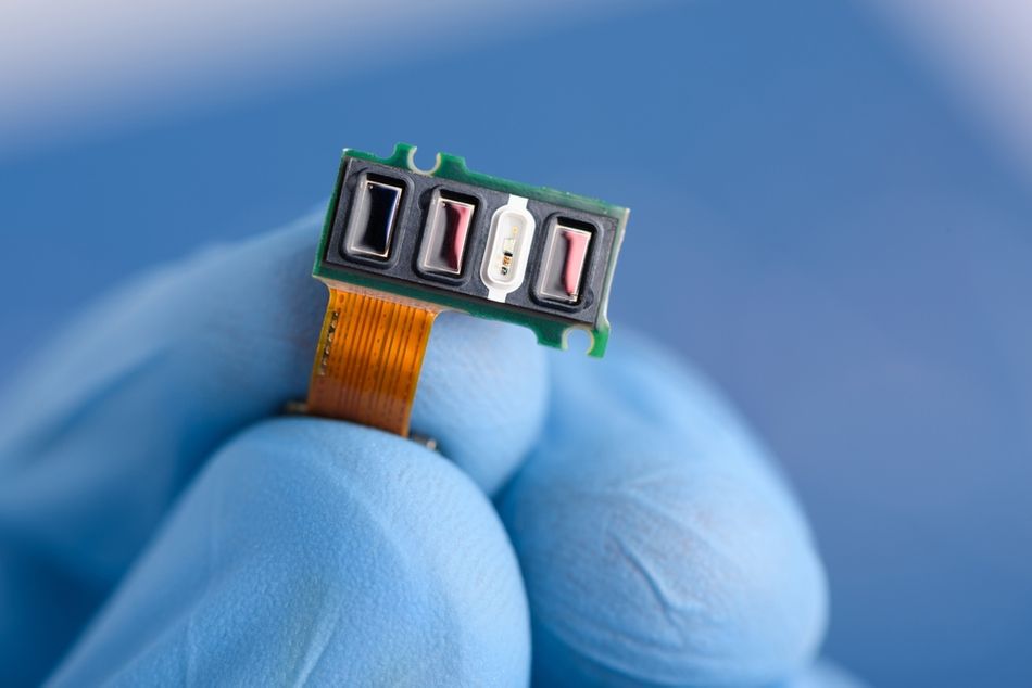
Optical Micro-Electro-Mechanical Systems (MEMS) Sensor
Introduction
Micro-Electro-Mechanical Systems (MEMS) sensors are revolutionizing modern technology by bridging the gap between the physical and digital worlds. These miniature marvels, typically ranging from micrometres to millimetres in size, integrate mechanical elements, sensors, actuators, transducers, and electronics on a single chip. MEMS sensors are used to measure physical quantities such as pressure, temperature, acceleration, and magnetic fields.
MEMS sensors play a vital role in our daily lives, silently working behind the scenes in our smartphones, automobiles, medical devices, and countless other applications. They enable the creation of highly sensitive, compact, and low-power devices, used in automotive safety systems, navigation, and environmental monitoring.
The MEMS sensors market is experiencing rapid growth, driven by increasing demand for high-performance, low-power, and cost-effective sensing solutions across multiple industries. By understanding the power of MEMS sensors, we gain a glimpse into the future of a world increasingly driven by intelligent and interconnected devices.
The Miniature Marvels: Unveiling MEMS Sensor Technology
What Makes MEMS Sensors Tick?
MEMS sensors are microscale devices that convert physical phenomena into electrical signals. These tiny marvels act as the "eyes and ears" of many modern devices, allowing them to sense and measure the physical world around us.
The operation of MEMS sensors relies on various sensing mechanisms, including capacitive, piezoresistive, and resonant sensing. Here’s their basic detail:
Capacitive MEMS sensors detect changes in capacitance due to the displacement of microstructures.
Piezoresistive sensors measure resistance changes in response to applied stress.
Resonant sensors exploit shifts in resonant frequency caused by external stimuli.
The core components of MEMS sensors work together to translate physical phenomena into a usable electrical signal. These include mechanical elements, sensing elements, and signal-processing circuits. Here's a breakdown of their roles:
Mechanical elements, such as cantilevers, diaphragms, and proof masses, interact with the environment and translate physical inputs into measurable displacements.
Sensing elements, often integrated with the mechanical structures, convert these displacements into electrical signals.
Signal processing circuits amplify, filter, and digitize the sensor output for further processing.
MEMS sensors offer significant advantages over traditional sensors. Here are some of those:
Their miniature size, typically ranging from 1 to 100 micrometres, allows for integration into compact devices. [1]
Low power consumption, often in the μW to mW range, makes them ideal for battery-powered applications.
High sensitivity enables precise measurements, with some inertial sensors achieving sub-μg resolution for accelerometers and sub-°/hour bias instability for gyroscopes.
By understanding the intricate interplay between micromechanics, transduction, and signal processing, we gain a deeper appreciation for the remarkable capabilities of MEMS sensors. These miniature marvels are transforming numerous industries and shaping the future of technology by enabling ever-smarter and more interconnected devices.
The Microscopic Manufacturing Marvel
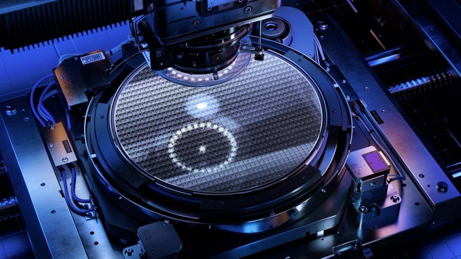
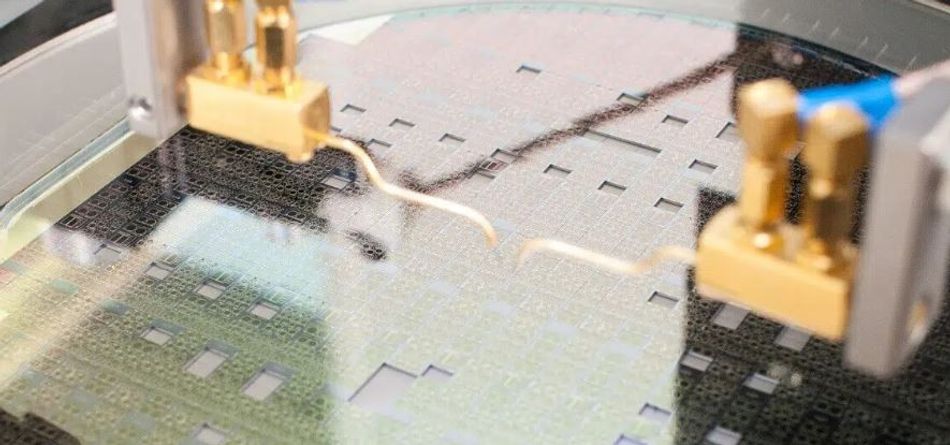
MEMS sensor fabrication is a complex process that combines traditional semiconductor manufacturing techniques with specialized micromachining methods, enabling batch production and cost-effective scaling. This approach also facilitates the integration of sensing elements with signal conditioning and processing circuitry on a single chip, reducing noise and improving overall performance. The two primary approaches are:
Surface micromachining involves depositing and patterning thin films on a substrate to create 3D structures.
Bulk micromachining selectively removes material from the substrate to form mechanical elements.
Photolithography is a crucial step in MEMS fabrication. It uses light-sensitive photoresists (positive or negative) to transfer patterns onto the substrate. Advanced exposure methods like deep-UV lithography and e-beam lithography enable feature sizes down to nanometers. [2] Following pattern transfer, etching processes remove material to create the desired structures.
- Wet etching uses chemical solutions like potassium hydroxide (KOH) for anisotropic etching of silicon.
- Dry etching techniques such as reactive ion etching (RIE) and deep reactive ion etching (DRIE) offer high aspect ratios and precise control.
Wafer bonding enables the creation of complex, multi-layered structures and sealed cavities that are essential for many MEMS sensor functionalities. Here's a breakdown of the different bonding techniques:
Anodic bonding joins silicon to glass using high voltage and temperature. This technique is particularly useful for creating sealed cavities in MEMS sensors, such as those used in pressure sensors.
Fusion bonding directly bonds silicon wafers at high temperatures. This technique is advantageous for its simplicity and creation of a very strong, hermetic seal.
Eutectic bonding uses intermediate metal layers to create strong bonds at lower temperatures. It offers the advantage of lower processing temperatures compared to fusion bonding, making it more suitable for situations where high temperatures might be detrimental.
Manufacturing at the microscale presents unique challenges.
- Stiction, the unintended adhesion of microstructures, is mitigated through anti-stiction coatings or critical point drying.
- Residual stress in deposited films can cause warping or deformation, addressed by careful material selection and stress-relief techniques.
- Process variability is managed through tight control of parameters and statistical process control.
MEMS fabrication requires stringent clean room conditions, typically class 100 (ISO 5) or better, to minimize particle contamination. Temperature, humidity, and vibration must be tightly controlled. Despite these precautions, yield rates in MEMS production can vary widely depending on device complexity. Simple devices may achieve yields over 90%, while complex, multi-layer devices might see yields of 50 - 70%. Continuous process optimization and design-for-manufacturability techniques are crucial for improving yields and reducing costs in MEMS sensor production.
Recommended Reading: What is a Sensor? An In-Depth Exploration and Comprehensive Guide
Sensing the World: MEMS Sensor Types and Applications
Inertial Sensors: Motion in Miniature
MEMS inertial sensors, comprising accelerometers and gyroscopes, are fundamental components in motion sensing applications. Accelerometers measure linear acceleration, while gyroscopes detect angular velocity. These sensors exploit different physical principles to achieve high-precision measurements in compact packages.
MEMS accelerometers primarily use capacitive or piezoresistive sensing mechanisms. Capacitive accelerometers feature a proof mass suspended between fixed electrodes, forming a differential capacitor. Acceleration causes the proof mass to deflect, changing the capacitance, which is then converted to an electrical signal. Piezoresistive accelerometers use strain gauges on a cantilever beam, where acceleration-induced stress changes the electrical resistance. [3]
MEMS gyroscopes commonly employ tuning fork or vibrating ring designs. Tuning fork gyroscopes use two masses vibrating in opposite directions. When rotated, the Coriolis effect causes a secondary vibration perpendicular to the drive axis, which is detected capacitively. Vibrating ring gyroscopes use a resonating ring structure, where rotation induces precession, detected as changes in capacitance between the ring and surrounding electrodes.
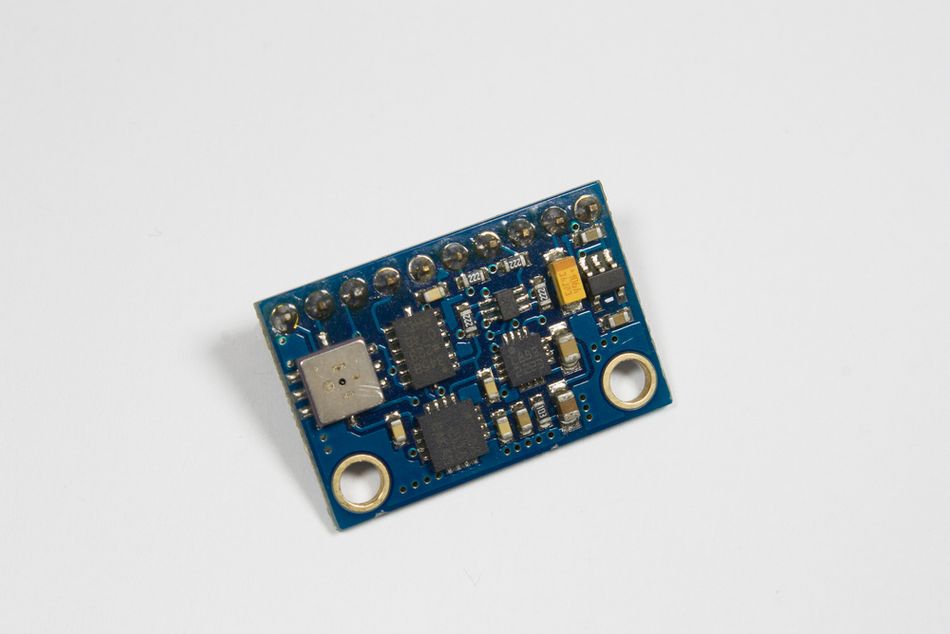
Inertial measurement unit (IMU) sensors are based on multiaxis combinations of precision gyroscopes, accelerometers, magnetometers, and pressure sensors. These plug-and-play solutions include full factory calibration, embedded compensation and sensor processing, and a simple programmable interface.
These inertial sensors find extensive applications in consumer electronics, automotive systems, and industrial equipment. In smartphones and wearables, they enable screen rotation, step counting, and gesture recognition. Automotive applications include electronic stability control, rollover detection, and airbag deployment systems. In industrial settings, they're crucial for inertial navigation systems in autonomous vehicles and drones.
Technical specifications of MEMS inertial sensors have improved significantly over the years. Modern MEMS accelerometers offer measurement ranges from ±2g to ±16g, with bandwidths up to several kHz and noise densities as low as 15 μg/√Hz. [4] MEMS gyroscopes typically provide measurement ranges from ±250°/s to ±2000°/s, with bandwidths up to 8 kHz and noise densities around 0.004 °/s/√Hz.
Signal processing plays a crucial role in enhancing the performance of inertial MEMS sensors. Here are some basic techniques used:
Oversampling techniques improve resolution and reduce noise by taking multiple measurements and averaging the results.
Temperature compensation algorithms correct for thermal drift, ensuring accurate measurements across a wide temperature range.
Kalman filtering is often employed to fuse data from multiple sensors, providing more accurate estimates of position and orientation.
These advanced signal processing techniques, often implemented on integrated digital signal processors, enable MEMS inertial sensors to achieve performance levels approaching those of much larger and more expensive fibre optic and ring laser gyroscopes.
Optical MEMS: Manipulating Light
Optical MEMS devices leverage microfabrication techniques to create miniature optical components that can manipulate light at the microscale. Two key elements in this field are micromirrors and microspectrometers, each employing unique working principles to achieve precise optical control.
Micromirrors in optical MEMS typically utilize either electrostatic or electromagnetic actuation. Electrostatically actuated micromirrors employ a torsional hinge design, where an applied voltage creates an electrostatic force that tilts the mirror. These mirrors can achieve switching speeds of up to 10 kHz. Electromagnetic actuation, on the other hand, uses current-carrying coils and permanent magnets to generate torque, offering larger deflection angles but at lower speeds, typically around 1 kHz.
Microspectrometers in MEMS come in two primary designs: grating-based and Fabry-Perot. Grating-based micro spectrometers use a diffraction grating to disperse light, which is then detected by a photodetector array. These devices can cover a wide spectral range from ultraviolet to near-infrared (200-2500 nm). [5] Fabry-Perot microspectrometers employ a tunable optical cavity, where the cavity length determines the transmitted wavelength. They offer high spectral resolution, typically 0.1-10 nm, but over a narrower spectral range.
Optical MEMS find diverse applications across multiple industries. In digital light processing (DLP) projectors, arrays of micromirrors rapidly switch to create images, operating at speeds up to 32 kHz. Optical switches in telecommunications use MEMS mirrors to route optical signals, achieving switching times under 10 ms. In spectroscopy, MEMS-based devices enable portable, high-resolution spectrometers for on-site chemical analysis, covering wavelengths from visible to mid-infrared (400-4000 nm).
In emerging technologies, optical MEMS play a crucial role in LiDAR systems for autonomous vehicles. MEMS-based scanning LiDAR uses rapidly oscillating micromirrors to steer laser beams, achieving scanning rates of 10-100 Hz. These systems can offer range resolutions better than 5 cm and detection ranges up to 200 meters, crucial for accurate environmental mapping in autonomous navigation.
The choice of materials is critical in optical MEMS. Polysilicon is commonly used for its good mechanical properties and compatibility with standard CMOS processes. It offers a refractive index of about 3.5 and can be shaped into complex structures. Aluminum is preferred for its high reflectivity (>90% in the visible spectrum) and is often used as a coating for micromirrors. For specific applications, materials like silicon nitride (for its high refractive index of ~2.0) or gold (for its excellent infrared reflectivity) are employed.
The selection of these materials and their precise fabrication enable optical MEMS devices to achieve the necessary optical properties, such as reflectivity, transmittance, and wavelength selectivity, crucial for their diverse applications.
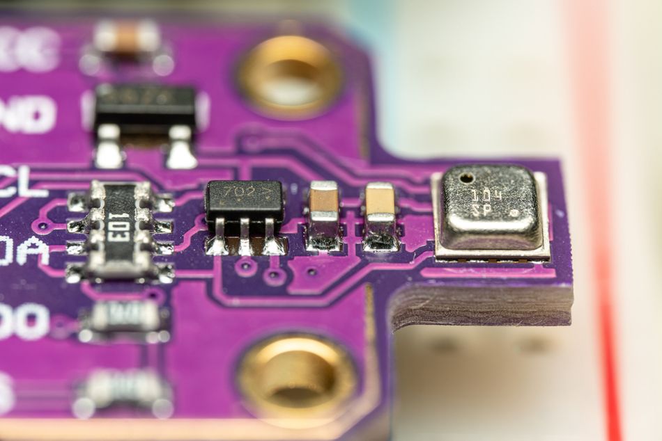
MEMS microphones, magnetometers, and pressure sensors are just a few examples of the many different types of MEMS sensors available. MEMS sensors are having a major impact on a wide range of industries, and they are sure to play an even greater role in the future.
Interfacing with the Macro World
Interfacing MEMS sensors with macroscale systems presents unique challenges due to the disparity in scale and signal characteristics. One primary challenge is impedance matching, as the high-impedance outputs of many MEMS sensors must be matched to lower-impedance inputs of standard electronic systems. This mismatch can lead to signal attenuation and increased susceptibility to noise. Additionally, the low-level signals produced by MEMS sensors are particularly vulnerable to electromagnetic interference (EMI) and radio-frequency interference (RFI), necessitating careful shielding and grounding techniques.

Signal conditioning is crucial for extracting accurate measurements from MEMS sensors. For capacitive sensors, charge amplifiers are commonly employed. These amplifiers convert the small changes in capacitance to voltage signals, providing high sensitivity and low noise. The output voltage (Vout) is related to the change in capacitance (ΔC) by the equation:

where Vref is the reference voltage and Cf is the feedback capacitance. For piezoresistive sensors, Wheatstone bridge circuits are typically used. These bridges convert small resistance changes to voltage differences, which can then be amplified. The bridge output voltage (Vout) is given by:

where Vex is the excitation voltage, ΔR is the resistance change, and R is the nominal resistance.
Analog-to-digital conversion (ADC) is a critical step in interfacing MEMS sensors with digital systems. Sigma-delta (ΣΔ) ADCs are particularly well-suited for MEMS applications due to their high resolution and excellent noise performance. These ADCs use oversampling and noise-shaping techniques to achieve resolutions of up to 24 bits. For example, a typical MEMS accelerometer might use a 16-bit ΣΔ ADC with an oversampling ratio of 64, providing an effective resolution of 0.05 mg over a ±2g range.
Common interface protocols for MEMS sensors include I2C (Inter-Integrated Circuit) and SPI (Serial Peripheral Interface). I2C is a two-wire interface that allows multiple devices to be connected to the same bus. It typically operates at data rates of 100 kHz (standard mode) or 400 kHz (fast mode), with some modern devices supporting up to 3.4 MHz. SPI, on the other hand, is a four-wire interface that offers higher speed and full-duplex communication. SPI can operate at data rates up to several MHz, making it suitable for high-bandwidth MEMS sensors like gyroscopes.
Real-world environments can introduce various factors that can affect the accuracy of MEMS sensor readings. These factors might include temperature fluctuations, power supply variations, or ageing effects. To mitigate these influences, calibration and compensation techniques are often employed:
Calibration: This involves exposing the sensor to known reference values of the physical parameter it measures (e.g., pressure, acceleration) and recording the corresponding electrical output. This data is used to create a mathematical model that can be applied to raw sensor readings to compensate for systematic errors.
Compensation: Microcontrollers or external circuitry can implement algorithms to adjust the sensor readings in real time based on factors like temperature readings from additional sensors integrated within the system.
By effectively interfacing MEMS sensors with the macro world, we unlock their vast potential to revolutionize various industries. From enabling the next generation of wearables and smartphones to creating smarter infrastructure and monitoring systems, the possibilities are endless.
Recommended Reading: Types of Sensors in Robotics
Pushing the Boundaries: Challenges and Innovations in MEMS Sensors
Overcoming Physical Limitations
MEMS sensors face several fundamental physical limitations that challenge their performance. Brownian noise, caused by the random motion of particles, sets a lower limit on the detectable signal in many MEMS devices. For inertial sensors, this noise floor is typically on the order of 50 ng/√Hz for accelerometers and 0.002 °/s/√Hz for gyroscopes. Thermo-mechanical noise, resulting from the coupling between thermal fluctuations and mechanical modes, further contributes to measurement uncertainty. In MEMS resonators, this noise manifests as phase noise, limiting frequency stability.
Allan variance, a measure of frequency stability over time, reveals long-term drift in inertial sensors. High-performance MEMS gyroscopes achieve bias instability around 0.1-1 °/hour, while tactical-grade devices reach 0.01 °/hour. However, these values are still orders of magnitude higher than the theoretical limit set by fundamental noise processes.
Advanced techniques are being employed to push MEMS sensor performance closer to theoretical limits. Vacuum packaging, which reduces air damping and thermal noise, has enabled quality factors exceeding 1 million in resonant devices. Electrostatic tuning allows for post-fabrication adjustment of sensor parameters, compensating for manufacturing variations and environmental effects. Mode-matching in resonant sensors, where drive and sense modes are precisely aligned, significantly enhances sensitivity and reduces noise.
Ongoing research is exploring novel materials to enhance MEMS sensor capabilities. Graphene, with its exceptional mechanical and electrical properties, shows promise for ultra-sensitive force and pressure sensors. Single-crystal diamond MEMS resonators have demonstrated quality factors exceeding 1 billion, offering unprecedented frequency stability. Quantum sensing techniques, such as optomechanical coupling in MEMS devices, are being investigated to surpass classical measurement limits.
The theoretical performance limits of MEMS sensors are determined by fundamental physical principles. For example, the quantum limit for force sensing is on the order of 10^-21 N/√Hz at room temperature. While current MEMS force sensors are still several orders of magnitude away from this limit, the gap is narrowing. In inertial sensing, the theoretical limit for angular random walk is around 10^-5 °/√hour, a target that advanced MEMS gyroscopes are approaching within an order of magnitude.
Recommended Reading: Sensor Fusion: The Ultimate Guide to Combining Data for Enhanced Perception and Decision-Making
The Next Generation: Emerging MEMS Technologies
Bio-MEMS represent a frontier in medical diagnostics and treatment. Lab-on-a-chip devices integrate multiple laboratory functions on a single chip, enabling rapid, point-of-care diagnostics. These systems can detect biomarkers at concentrations as low as femtomolar (10^-15 M), rivalling traditional laboratory techniques. Implantable bio-MEMS, such as glucose sensors and drug delivery systems, offer continuous monitoring and precise dosing, potentially revolutionizing the management of chronic diseases.
RF MEMS are transforming wireless communication systems. MEMS-based tunable capacitors achieve quality factors exceeding 100 at GHz frequencies, enabling agile and efficient RF front-ends. MEMS switches demonstrate insertion losses below 0.1 dB and isolation better than 40 dB up to 40 GHz, outperforming solid-state alternatives. These devices are crucial for the development of reconfigurable antennas and adaptive RF systems in 5G and beyond.
Energy harvesting MEMS are addressing the power needs of IoT devices and wireless sensor networks. Piezoelectric MEMS harvesters can generate power densities up to 500 μW/cm³ from vibrations, while thermoelectric MEMS achieve efficiencies around 5-10% for small temperature gradients. These technologies enable self-powered sensors for structural health monitoring, wearable devices, and environmental sensing.
The impact of these emerging MEMS technologies is far-reaching. In healthcare, bio-MEMS are enabling personalized medicine and early disease detection. RF MEMS are facilitating the development of software-defined radios and cognitive wireless networks. Energy harvesting MEMS are paving the way for autonomous sensor networks in smart homes and industrial automation applications.
Fabrication challenges for these advanced MEMS include achieving precise control over nanoscale features, integrating heterogeneous materials, and ensuring long-term reliability. Novel materials such as piezoelectric aluminium nitride, high-k dielectrics, and shape memory alloys are being incorporated to enhance device performance. Additive manufacturing techniques, including 3D printing at the microscale, are opening new possibilities for complex MEMS structures.
Current research is focusing on integrating MEMS with advanced electronics and photonics. For instance, MEMS-on-CMOS integration enables smart sensors with on-chip signal processing and machine learning capabilities. Optomechanical MEMS, combining mechanical elements with photonic structures, are pushing the boundaries of sensing and quantum information processing.
Recommended Reading: Novel Circuit Design Approach Makes Pressure Sensors Smaller and More Sensitive
Conclusion
MEMS sensors have solidified their place as a revolutionary force in modern technology. Their miniature size, high performance, and cost-effectiveness have transformed countless industries. From smartphones to automobiles and medical devices, MEMS microsensors are everywhere. Ongoing research delves deeper into miniaturization, materials, and integration, promising a future brimming with potential. These tiny marvels will undoubtedly play a pivotal role in shaping a smarter, more interconnected world, where technology seamlessly integrates into every aspect of our lives.
Frequently Asked Questions
Q. What is the difference between MEMS sensors and traditional sensors?
A. MEMS sensors integrate mechanical and electrical components on a single chip, offering smaller sizes, lower power consumption, and often better performance than traditional sensors.
Q. What are the main challenges in designing and manufacturing MEMS sensors?
A. Key challenges include achieving high yield at microscale, managing residual stresses, ensuring hermetic packaging, and integrating with CMOS electronics efficiently.
Q. Can MEMS sensors be used in harsh environments?
A. Yes, with specialized packaging and materials, MEMS sensors can operate in extreme temperatures, pressures, and even radiation environments.
Q. How do MEMS sensors contribute to the Internet of Things (IoT)?
A. MEMS sensors enable key IoT functionalities like environmental monitoring, motion sensing, and location awareness, with 41 billion units expected in IoT devices by 2025.
Q. What is the expected market growth for MEMS sensors?
A. The MEMS Sensor Market size is estimated at USD 17.18 billion in 2024, and is expected to reach USD 26.65 billion by 2029.
References
[1] ResearchGate. MEMS Based Sensors – A Comprehensive Review of commonly used Fabrication Techniques [Cited 2024 July 12] Available at: Link
[2] NCBI. Evolution in Lithography Techniques: Microlithography to Nanolithography [Cited 2024 July 12] Available at: Link
[3] ResearchGate. Piezoresistive Strain Gauges for Use in Wireless Component Monitoring Systems [Cited 2024 July 12] Available at: Link
[4] Analog Devices. MEMS Accelerometers for Condition Monitoring [Cited 2024 July 12] Available at: Link
[5] MDPI. Design and Fabrication of Silicon-Blazed Gratings for Near-Infrared Scanning Grating Micromirror [Cited 2024 July 12] Available at: Link
Table of Contents
IntroductionThe Miniature Marvels: Unveiling MEMS Sensor TechnologyWhat Makes MEMS Sensors Tick?The Microscopic Manufacturing MarvelSensing the World: MEMS Sensor Types and ApplicationsInertial Sensors: Motion in MiniatureOptical MEMS: Manipulating LightInterfacing with the Macro WorldPushing the Boundaries: Challenges and Innovations in MEMS SensorsOvercoming Physical LimitationsThe Next Generation: Emerging MEMS TechnologiesConclusionFrequently Asked QuestionsReferences