PCBA Manufacturing: Revolutionizing Modern Electronics Assembly
Discover the latest advancements in PCBA manufacturing and how they are transforming the electronics industry. Learn about foundational concepts, innovative technologies, real-world applications, and challenges in this comprehensive guide.

18 Jun, 2024. 14 minutes read
Introduction
PCBA (Printed Circuit Board Assembly) manufacturing is a crucial process in the electronics industry, involving the assembly of electronic components onto a PCB (Printed Circuit Board). This process transforms bare PCBs into functional units that power a wide array of electronic devices. PCBA manufacturing underpins the production of everything from consumer electronics like smartphones and laptops to critical medical devices and industrial automation systems.
As technology advances, PCBA manufacturing continues to evolve, enhancing the efficiency, reliability, and performance of electronic products. Its has a profound impact on the engineering field, driving innovation and enabling the development of increasingly sophisticated and compact electronic systems.
Understanding PCBA: Key Concepts and Basics
What is PCBA?
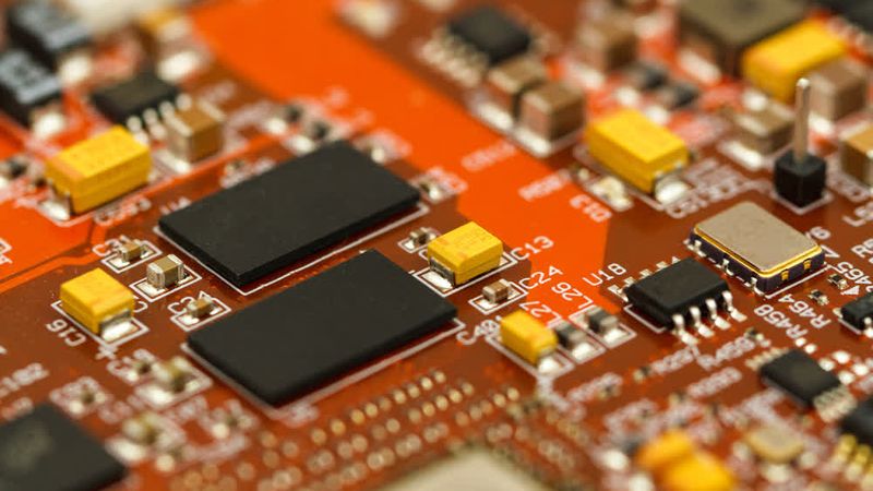
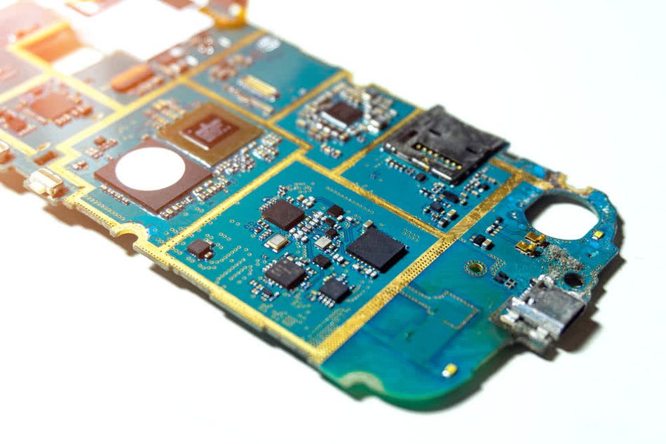
Printed Circuit Board Assembly (PCBA) is the process of soldering or assembling electronic components onto a printed circuit board (PCB). This results in a functional electronic circuit that can perform specific tasks as designed. The PCBA process is essential in the production of electronic devices. It enables the integration of various components such as microchips, resistors, and capacitors onto a single board.
PCBs (Printed Circuit Boards) serve as the foundation for PCBA. A PCB is a non-conductive substrate, typically made of fibreglass, composite epoxy, or other laminate materials, which provides physical support and wiring for the surface-mounted and socketed components.
Difference Between PCB and PCBA
While PCB and PCBA may sound similar and are often used interchangeably, there are a couple of key differences between them:
A PCB is the bare board, while a PCBA is the completed assembly that includes all the electronic components.
PCBs are mostly manufactured through fabrication while PCBAs are assembled with machines or manually.
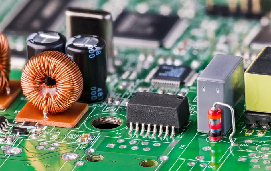
Typically, a PCBA consists of the following electronic components, while a PCB is just a plain board with traces and vias.
Resistors: Components that limit the flow of electrical current within a circuit.
Capacitors: Devices that store and release electrical energy.
Integrated Circuits (ICs): Miniaturized electronic circuits that consist of semiconductor devices and passive components.
Connectors: Interfaces that allow the PCBA to connect with other devices or components, enabling the transfer of electrical signals.
Diodes: Semiconductor devices that allow current to flow in one direction only.
Transistors: Semiconductor devices used to amplify or switch electronic signals.
Further Reading: PCBA vs PCB: The foundation of modern-day electronics
Types of PCBA Technologies
Printed Circuit Board Assembly process works on two basic technologies, i.e.
Surface Mount Technology (SMT)
Through-Hole Technology (THT)
Surface Mount Technology
Surface-mount technology (SMT) is a game-changer for electronics. Tiny, delicate components like transistors are soldered directly onto the board's surface, eliminating drilling and saving space. It supports double-sided assembly, which shrinks the overall PCB size and also speeds up production.
Through-Hole Technology
Through-Hole Technology (THT) is an older technology than SMT, and it offers a strong connection. Components with wires are plugged through holes in the board and soldered. This takes more time than SMT, but THT is the go-to option for hefty components like high-power coils and capacitors that need to handle stress.
Further Reading: SMT Assembly vs. Through-Hole: What to Know
The PCBA Process: Step-by-Step
The PCBA process varies from technology to technology. The initial design and layout process is pretty similar barring the use of SMD and through hole solder pads for the respective process.
However, there are a few differences at the soldering and component placement stages.
Design and Layout
The process begins with designing the PCB layout using CAD (Computer-Aided Design) software. Engineers create detailed schematics, defining the placement of components and the routing of electrical connections. This step sets the foundation for the entire manufacturing process, ensuring that the final product meets design specifications and functionality.
PCB Printing
The PCB design is transferred onto a physical board. This involves printing the circuit pattern onto copper-clad laminate sheets using techniques like photolithography. This process is borrowed from semiconductor manufacturing for precise and intricate circuit patterns.
For SMT PCBAs
Solder Paste Application
Solder paste is applied to the board using a stencil that matches the PCB layout. This paste contains tiny balls of solder suspended in a flux, which helps in creating electrical connections. Accurate application of solder paste is vital to avoid defects like solder bridges and insufficient solder, which can lead to poor connections.
Suggested Reading: Types of Solder: A Comprehensive Guide for Engineering Professionals
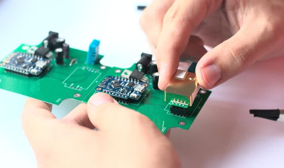
Component Placement
Automated machines called pick-and-place machines use precise coordinates from the design files to place each component accurately. Such modern machines can place thousands of components per hour with high precision.
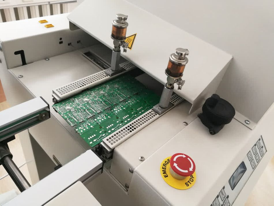
Reflow Soldering
The PCB with the components is passed through a reflow oven. In this oven, the solder paste melts and solidifies, creating secure electrical connections between the components and the PCB. Reflow soldering has evolved significantly, with advanced ovens now featuring precise temperature controls to ensure consistent and reliable solder joints.
Inspection and Quality Control
The PCBA is then inspected through Automated Optical Inspection (AOI) systems to check for defects such as:
Solder bridgesMissing components
Component misalignments.
Likewise, X-ray inspection may also be used to examine hidden solder joints to identify and rectify issues before the final product assembly.
For THT PCBAs
Through-Hole Component Insertion
Through-hole components are inserted either manually or using automated insertion machines. The components' leads pass through holes in the PCB and are soldered to the designated pads on the opposite side. This method ensures robust mechanical and electrical connections, essential for components that handle higher currents.
Wave Soldering
The PCB is passed over a wave of molten solder, which adheres to the exposed metal areas and component leads, forming strong connections. Wave soldering is particularly effective for boards with a high density of through-hole components, providing reliable solder joints quickly and efficiently.
Functional Testing
The final step is functional testing, where the completed PCBA is tested to ensure it operates as intended. This may involve in-circuit testing (ICT), where electrical probes test the functionality of various components, or functional testing, which checks the board's performance under real-world conditions.
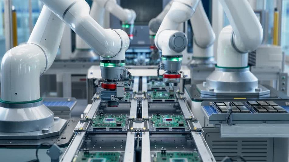
Automation and Robotics in PCBA
Automation and robotics have revolutionized PCBA manufacturing by significantly increasing efficiency, precision, and reliability. These technologies streamline various stages of the manufacturing process, from component placement to inspection, ensuring high-quality outputs with minimal human intervention.
Robotic systems used in PCBA manufacturing include: *
Pick-and-place machines
Automated optical inspection (AOI) systems
Soldering robots.
Pick-and-place machines precisely position surface mount components on PCBs, using high-speed vision systems and precise motion control to handle thousands of components per hour.
Suggested Reading: No Code Robotics Enable Automation For Everyone
The software used in these robotic systems plays a crucial role in their operation. Advanced algorithms and machine learning techniques enable these systems to optimize placement sequences, detect and correct misalignments, and adapt to variations in component shapes and sizes.
For instance, AOI systems use sophisticated image processing software to inspect solder joints and component placements, identifying defects that might be missed by human inspectors.
Key Benefits of Automation and Robotics in PCBA Manufacturing
Increased Throughput: Robotic systems can operate continuously without fatigue, handling large volumes of work at speeds unattainable by human workers.
Enhanced Precision: Automation ensures consistent and precise placement of components, reducing the risk of errors.
Improved Quality Control: Automated inspection systems provide thorough and consistent quality checks, identifying defects early in the production process.
Cost Efficiency: While the initial investment in robotics and automation can be high, the long-term savings from increased efficiency and reduced labor costs are substantial.
Flexibility: Modern robotic systems can be quickly reprogrammed to handle different products or adapt to changes in design, providing significant flexibility in manufacturing operations.
These advancements have not only improved the quality and reliability of PCBAs but have also enabled manufacturers to meet the growing demand for complex and miniaturized electronic devices.
Material Innovations
Material innovations are at the forefront of advancements in PCBA manufacturing, driving improvements in performance, reliability, and versatility of electronic assemblies. Two significant areas of development are advanced substrates and conductive inks.
Advanced Substrates
The substrate is the foundational material of a PCB, and recent innovations have led to the development of high-performance substrates that enhance the capabilities of electronic assemblies.
Material | Properties | Applications |
Polyimide Substrates | Excellent thermal resistance and flexibility, ideal for high-temperature applications and flexible PCBs | Military and Aerospace applications. |
Rogers Materials | Excellent dielectric properties, low-signal loss, and high frequency performance | RF and microwave applications in communication and radar systems. |
Copper or aluminum core for enhanced thermal conductivity. | LED lighting and power electronics. |
Suggested Reading: What are Circuit Boards Made Of? An Extensive Guide to Materials and Manufacturing Processes
Conductive Inks
Conductive inks are another breakthrough in PCBA materials, allowing for new manufacturing techniques and more versatile applications. These inks contain conductive materials such as silver, copper, or carbon, and can be printed onto substrates to form electrical circuits.
Type of Ink | Properties | Applications |
Silver Conductive Inks | High conductivity, fine lines & patterns, excellent reliability | Touchscreens, flexible displays, printed electronics |
Copper Conductive Inks | Cost-effective alternative, improved oxidation resistance & conductivity | RFID tags, antennas, cost-sensitive applications |
Carbon Conductive Inks | Flexible, durable, lower conductivity | Printed sensors, electrodes, applications needing stability & cost-effectiveness |
These material innovations are not only enhancing the performance and capabilities of PCBAs but also enabling new manufacturing methods and applications, driving the evolution of modern electronics.
Practical Applications of PCBA
Consumer Electronics
Printed Circuit Board Assemblies (PCBAs) are pivotal for the manufacturing of consumer electronics, providing the essential platform for assembling complex electronic circuits. These assemblies ensure that various electronic components, such as microprocessors, memory chips, and sensors, are interconnected and function cohesively.
Smartphones: In smartphones, PCBAs house the central processing unit (CPU), memory, power management ICs, and communication modules. A typical smartphone PCBA includes components like:
Processor - Multi-core CPUs that manage the phone's operations.
Memory - Flash memory chips for data storage and RAM for temporary data access.
Power Management ICs - Regulate battery charging and power distribution.
Communication Modules - LTE/5G, Wi-Fi, and Bluetooth chips for connectivity.
Case Study: The Apple iPhone X features a highly integrated PCBA that includes the A11 Bionic chip, a 64-bit six-core CPU with a neural engine for advanced AI processing. This design allows for enhanced performance and energy efficiency, boosting the speed by 30 percent from its predecessors, demonstrating the critical role of PCBA in enabling cutting-edge technology.
Laptops: In laptops, PCBAs support the main motherboard, connecting the CPU, GPU, memory, storage devices, and peripheral interfaces. Key technical specifications for laptop PCBAs include:
Processor - High-performance CPUs such as Intel Core i7 or AMD Ryzen.
Graphics - Dedicated GPUs like NVIDIA GeForce or integrated graphics solutions.
Storage - SSDs for fast data access and storage.
Connectivity - USB, HDMI, Ethernet, and wireless modules.
Case Study - The Dell XPS 15 utilizes a PCBA with the Intel Core i7 processor and NVIDIA GeForce RTX 40 Series GPUs. This combination provides robust performance for both professional applications and gaming, highlighting the versatility and power of modern PCBA designs in laptops.
Wearable Devices: Wearable devices, such as smartwatches and fitness trackers, rely on miniaturized PCBAs to integrate various sensors, processors, and communication modules within a compact form factor. Essential components include:
Microcontroller - Manages device operations and sensor data processing.
Sensors - Accelerometers, gyroscopes, and heart rate monitors.
Connectivity - Bluetooth and Wi-Fi modules for data transmission.
Case Study: The Fitbit Charge 4 incorporates a PCBA that integrates a GPS module, heart rate monitor, and Bluetooth connectivity within a slim form factor with an extended battery life. The design showcases the ability of PCBAs to support multiple functions in a compact and wearable form.
Medical Industry
PCBA plays a pivotal role in transforming the designs for medical devices allowing to overcome the shortcomings in the healthcare sector.
Scanning and Tracking Devices: Typically, PCBA are used for producing small and large medical gadgets that may include heavy machines like MRI scanners, to sophisticated miniaturized sensors for monitoring patient vitals.
The demand for PCBA powered medical gadgets has continually increased creating a lucrative industry for manufacturers. With a digitised design, medical equipment like defibrillators, imaging systems, muscle stimulators, CT scans, and ultrasonic equipment enable a seamless interface for doctors to track and visualize patients and create instant digital reports.
Most of these equipment feature PCBA technology that supports the small form factor and seamless portability for these devices.
Artificial Limbs: Printed Circuit Board Assemblies (PCBAs) play a critical role in modern artificial limbs. These miniaturized circuit boards house the brains of the prosthetic, containing microprocessors, sensors, and actuators.
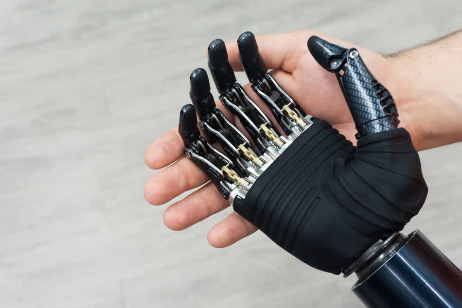
Fig 6: An artificial robotic limb
PCBAs interpret signals from the user's residual limb or external controls, translating them into movement commands for the prosthetic's motors. This allows for functionalities like natural gait patterns, adjustable resistance, and even sensory feedback in advanced prosthetics.
Case Study: The iLimb prosthetic hand developed by Touch Bionics utilizes a sophisticated PCBA with multiple microprocessors to control its various individual finger movements. Sensors detect muscle contractions in the residual limb, and the PCBA interprets these signals to provide users with intuitive and proportional control over the prosthetic hand. This advancement significantly improves dexterity and functionality for amputees.
Suggested Reading: Could this lifelike robotic hand be the start of a humanoid future?
Overcoming Challenges in PCBA Manufacturing
Quality Control and Testing
Quality control and testing are critical components in PCBA manufacturing, ensuring that the final products meet the required specifications and are free from defects. It helps prevent costly errors and improves the reliability and performance of electronic assemblies.
Automated Optical Inspection (AOI): AOI is a key testing method used to inspect PCBAs for defects. It uses high-resolution cameras to capture images of the board, which are then analyzed by specialized software to detect issues such as solder bridges, missing components, and incorrect placements.
Technical Details: AOI systems can inspect solder joints, component orientation, and markings with high precision. The software compares the captured images against the design specifications, highlighting any discrepancies.
Example: A typical AOI system can process hundreds of boards per hour, providing rapid feedback to the manufacturing line and allowing for immediate corrective actions.
X-ray Inspection: X-ray inspection is another essential testing method, particularly useful for detecting hidden defects in solder joints and multilayer PCBs. This non-destructive testing technique uses X-rays to penetrate the board and reveal internal structures.
Technical Details: X-ray inspection systems can identify issues such as voids in solder joints, insufficient solder, and internal cracks. They provide a 3D view of the board, allowing for comprehensive analysis.
Example: An X-ray inspection system can examine fine-pitch components and Ball Grid Arrays (BGAs), ensuring that even the most challenging connections are free from defects.
Further Reading: Automated inspection of PCBs
Key Quality Control Steps:
Pre-Production Testing - Design and material verification before full-scale production.
In-Process Inspection - Continuous assembly monitoring with AOI and inline testing methods to catch defects early.
Functional Testing - Testing the PCBA electrical functionality with in-circuit testing (ICT) and final functional testing.
Post-Production Analysis - Final inspection of the completed boards using X-ray inspection and other methods to verify the integrity of hidden solder joints.
Feedback and Improvement - Use data from quality control processes to identify areas for improvement in the manufacturing process. Implement corrective actions and refine procedures to enhance overall quality.
Supply Chain Management
Supply chain management in PCBA manufacturing directly impacts production efficiency, cost, and quality. Effective management ensures that all necessary components are available when needed, and that manufacturing processes can proceed without delays.
Challenges in Supply Chain Management:
Component Shortages - The electronics industry frequently faces shortages of critical components like semiconductors, resistors, and capacitors, which halts or delays the production process
Lead Times - Long lead times for procuring components can disrupt the production schedule. Factors such as global demand, supplier capacity, and logistical constraints contribute to these delays.
Quality Control - Ensuring the quality of components from various suppliers is challenging. Variability in component quality can lead to defects and rework, increasing costs and time.
Strategies for Mitigating Risks:
Supplier Management - Develop strong relationships with multiple suppliers to diversify the risk. Vet suppliers thoroughly to ensure they can meet quality and delivery requirements.
Inventory Control - Implement just-in-time (JIT) inventory systems to reduce the holding costs and minimize excess inventory. However, maintain a safety stock of critical components to buffer against shortages.
Forecasting and Planning - Use advanced forecasting tools to predict demand accurately. Align procurement strategies with production schedules to ensure timely component availability.
Technical Considerations:
Tracking Systems - Utilize advanced tracking systems like RFID and IoT-enabled sensors to monitor the location and status of components in real-time. This enhances visibility and helps in managing the supply chain more efficiently.
Data Analytics - Employ data analytics to analyze historical data and predict future trends. This aids in making informed decisions about procurement, inventory management, and supplier performance.
Quality Management Systems - Implement rigorous quality management systems to inspect and verify component quality upon receipt. Automated testing and inspection can ensure that only components meeting the required standards are used in production.
Conclusion
PCBA manufacturing is a cornerstone of modern electronics, driving innovation and efficiency across various industries. By integrating advanced materials, automation, and quality control measures, PCBA manufacturing ensures the production of reliable and high-performance electronic devices. From consumer electronics to industrial automation systems, the advancements in PCBA technology are pivotal in meeting the increasing demands for miniaturization, functionality, and cost-effectiveness. The continuous evolution of PCBA manufacturing techniques not only enhances product quality but also opens new avenues for technological breakthroughs in the electronics industry.
Frequently Asked Questions (FAQs)
What are the main components involved in PCBA?
The main components involved in PCBA (Printed Circuit Board Assembly) include:
Resistors: These components limit the flow of electrical current in a circuit, ensuring that other components operate within safe parameters.
Capacitors: Capacitors store and release electrical energy, playing crucial roles in filtering and power supply stabilization.
Integrated Circuits (ICs): ICs are compact semiconductor devices that can contain thousands to millions of electronic components such as transistors, diodes, and resistors, all interconnected to perform complex functions.
Connectors: Connectors provide the interface between the PCBA and other electronic components or systems, enabling communication and power transfer.
How do advancements in PCBA manufacturing impact the electronics industry?
Advancements in PCBA manufacturing have far-reaching implications for the electronics industry:
Increased Efficiency: Automation and robotics in PCBA manufacturing streamline the production process, reducing labor costs and increasing throughput.
Enhanced Precision: Advanced soldering techniques and quality control measures improve the accuracy and reliability of PCBAs, reducing the incidence of defects and rework.
Miniaturization: Innovations in materials and manufacturing techniques enable the production of smaller, more compact PCBAs, supporting the development of miniaturized electronic devices.
Cost Reduction: Improved manufacturing processes and material efficiency lead to lower production costs, making advanced electronic devices more affordable for consumers.
Innovation: Continuous advancements in PCBA technology drive innovation, allowing for the development of new electronic products with enhanced capabilities and performance.
What are common testing methods used in PCBA manufacturing?
Common testing methods used in PCBA manufacturing include:
Automated Optical Inspection (AOI): AOI uses high-resolution cameras and sophisticated software to inspect solder joints, component placements, and markings. It detects defects such as solder bridges, missing components, and misalignments.
X-ray Inspection: X-ray inspection is used to detect hidden defects within solder joints and multilayer PCBs. It can identify voids, insufficient solder, and internal cracks by providing a 3D view of the board's internal structures.
Functional Testing: Functional testing verifies that the assembled PCBA operates as intended. This includes in-circuit testing (ICT) to check the functionality of individual components and final functional testing to ensure the complete board performs under real-world conditions.
References
What is PCBA? Types, benefits, applications, assembly, and more - IBE Electronics (pcbaaa.com)
An Ultimate Guide to PCBA: Definition,Types, Applications, Process (mokotechnology.com)
Through Hole (TH) Technology: Everything You Need Know (nextpcb.com)
Apple iPhone X Explained: Features, Price, Specs, and More | Digital Trends
Fitbit Charge 4 review: A better fitness tracker without the bulk - CNET
Medical PCB - Applications and Types of PCBs for Medical Industry (absolutepcbassembly.com)
i-Limb - ROBOTS: Your Guide to the World of Robotics (robotsguide.com)
Table of Contents
IntroductionUnderstanding PCBA: Key Concepts and BasicsWhat is PCBA?Difference Between PCB and PCBATypes of PCBA TechnologiesSurface Mount TechnologyThrough-Hole TechnologyThe PCBA Process: Step-by-StepDesign and LayoutPCB Printing For SMT PCBAsSolder Paste ApplicationComponent PlacementReflow SolderingInspection and Quality Control For THT PCBAsThrough-Hole Component InsertionWave SolderingFunctional TestingAutomation and Robotics in PCBAKey Benefits of Automation and Robotics in PCBA ManufacturingMaterial InnovationsAdvanced Substrates Conductive Inks Practical Applications of PCBA Consumer ElectronicsMedical IndustryOvercoming Challenges in PCBA ManufacturingQuality Control and TestingSupply Chain ManagementConclusionFrequently Asked Questions (FAQs)References