SMD Package Types and Sizes: A Comprehensive Guide for Engineers
A Deep Dive into Types, Packages, Sizes, Applications in Modern Electronics, and the innovations in SMD technology that have revolutionized PCB design

04 Sep, 2024. 16 minutes read
No time now? Save for later.
We only use your email to send this link. Privacy Policy.
Introduction
Surface Mount Device (SMD) technology has revolutionized the electronics industry, enabling the creation of smaller, lighter, and more efficient devices. These are miniature components, much different from their conventional PCB component outlook, soldered directly onto the surface of printed circuit boards (PCBs).
SMD components have become the backbone of modern electronics manufacturing. The diverse array of SMD package types and sizes plays a crucial role in PCB design and manufacturing, allowing engineers to optimize space utilization, thermal management, and electrical performance. Understanding the nuances of SMD package variations is essential for engineers to make informed decisions in their designs, balancing factors such as power requirements, signal integrity, and cost-effectiveness.
The SMD Revolution: Shrinking Electronics
Surface Mount Technology (SMT) revolutionized electronic component assembly, superseding the traditional through-hole technology. In SMT, components are directly mounted onto the surface of printed circuit boards (PCBs), eliminating the need for lead insertion through holes. This fundamental change in assembly methodology has catalyzed a revolution in electronic device miniaturization and performance enhancement.
Why SMT Superseded Through Hole?
SMT offers several significant advantages over its predecessor.
Increased Packaging Density - The elimination of through holes allows for higher component density, resulting in more compact and lightweight devices. This increased packing density translates to shorter signal paths, reducing parasitic capacitance and inductance, thereby improving high-frequency performance and signal integrity.
Lower Lead Inductance - SMT components typically have lower lead inductance and resistance, contributing to enhanced electrical characteristics.
Compact Component Sizes - The ability to shrink component sizes has led to the proliferation of ultra-portable devices such as smartphones, wearables, and IoT sensors.
Fabrication of Complex Systems - SMD technology has enabled the integration of complex systems into ever-smaller form factors, pushing the boundaries of what's possible in fields like medical implants, aerospace, and automotive electronics.
Quicker Production - SMT only requires solder paste and doesn’t require any drilling for holes, so it improves the production time and reduces setup complexity.
Recommended Reading: SMT Assembly vs. Through-Hole: What to Know
From a manufacturing perspective, SMT offers increased automation potential, reducing assembly time and labor costs. The reflow soldering process used in SMT allows for simultaneous soldering of all components, improving throughput and yield. Additionally, SMT's reduced drill hole requirements simplify PCB design and manufacture, leading to cost savings and increased reliability.
Aspect | Surface Mount Technology (SMT) | Through-Hole Technology |
Component Size | Smaller (e.g., 0201, 01005 packages) | Larger |
Component Density | Higher | Lower |
Signal Path Length | Shorter | Longer |
Parasitic Effects | Reduced | Higher |
Assembly Process | Reflow soldering | Wave soldering or manual |
Automation Potential | High | Lower |
PCB Real Estate Utilization | More efficient | Less efficient |
Thermal Dissipation | Generally better | Limited by lead thermal resistance |
Mechanical Strength | Lower (but sufficient for most applications) | Higher |
High-Frequency Performance | Superior | Limited by lead inductance |
Cost-Effectiveness | Higher for high-volume production | Lower for low-volume production |
The adoption of SMT has necessitated advancements in pick-and-place machinery, solder paste technology, and inspection systems. Engineers must now consider factors such as tombstoning, solder bridging, and coplanarity in their designs.
Decoding SMD Package Nomenclature
Understanding SMD package nomenclature is crucial for engineers to accurately specify and identify components in electronic designs. The naming conventions for SMD packages typically consist of a combination of letters and numbers, each carrying specific information about the package's characteristics.
SMD package names often start with a prefix that indicates the general package type. For example:
SOT: Small Outline Transistor
SOIC: Small Outline Integrated Circuit
QFP: Quad Flat Package
Following the prefix, numbers and additional letters provide more detailed information about the package's dimensions, pin count, or specific variations. For instance, consider ‘SOT-23-5’
In this example:
SOT: Small Outline Transistor
23: Specific variant of the SOT family
5: Number of pins
Similarly, consider, ‘TQFP - 144’
Here:
T: Thin
QFP: Quad Flat Package
144: Number of pins
The significance of numbers can vary depending on the package type. They may represent:
Pin count
Package dimensions (e.g., body size or height)
Specific variants within a package family
Letters in package names often denote:
Package variations (e.g., "T" for Thin, "L" for Low profile)
Lead frame materials (e.g., "Cu" for Copper)
Special features (e.g., "EP" for Exposed Pad)
Here's a comprehensive table of common SMD package prefixes and their meanings:
Prefix | Full Name | Description |
BGA | Ball Grid Array | Array of solder balls on the bottom for high-density connections |
CSP | Chip Scale Package | Nearly as small as the die itself, typically for ICs |
DFN | Dual Flat No-lead | Small surface-mount package with no leads |
LGA | Land Grid Array | Similar to BGA, but with flat contacts instead of balls |
QFN | Quad Flat No-lead | Square package with terminals on four sides, no leads |
QFP | Quad Flat Package | Square package with gull-wing leads on four sides |
SOP | Small Outline Package | Rectangular package with gull-wing leads on two sides |
SOT | Small Outline Transistor | Typically used for transistors and small ICs |
TSOP | Thin Small Outline Package | Thinner version of SOP, often used for memory chips |
WCSP | Wafer-level Chip Scale Package | Extremely small package created at the wafer level |
When interpreting more complex package names, consider each part separately. For example, ‘eTQFP-144-1EP’
Breakdown:
e: Enhanced (often indicating better thermal performance)
TQFP: Thin Quad Flat Package
144: Number of pins
1EP: One Exposed Pad on the bottom for improved thermal dissipation
Mastering SMD package nomenclature allows engineers to quickly assess a component's physical characteristics, pin count, and special features, facilitating efficient PCB design and component selection processes.
SMD Package Types and Form Factors Chip Components: Resistors and Capacitors
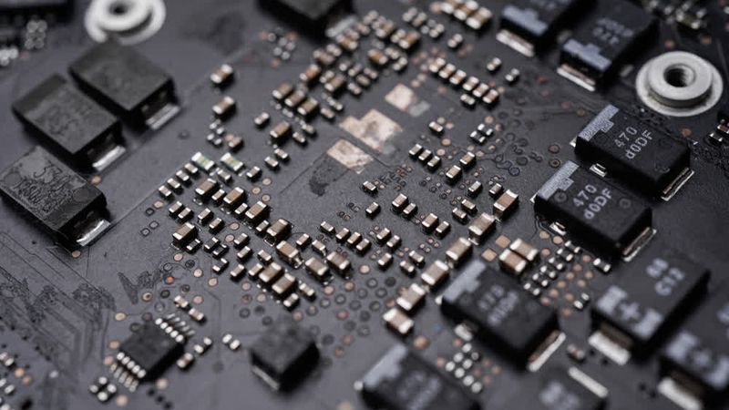
Chip resistors and capacitors are fundamental building blocks in modern electronic designs, offering compact and efficient solutions for surface mount technology (SMT) applications. These components are characterized by their rectangular shape and small form factors, allowing for high-density placement on printed circuit boards (PCBs).
The structure of chip components typically consists of a ceramic substrate with conductive end terminations. For resistors, a resistive element is deposited on the substrate.
Suggested Reading: SMD Resistor Sizes: A Comprehensive Guide for Engineers
On the other hand, capacitors use dielectric materials sandwiched between conductive plates. This design allows for efficient manufacturing and reliable performance in various electronic applications.
Chip components use a standardized sizing system that combines metric and imperial measurements. The sizing nomenclature, such as 0201, 0402, or 0603, represents the component's length and width in hundredths of inches. For example:
0201: 02 (0.02 inches) x 01 (0.01 inches)
0402: 04 (0.04 inches) x 02 (0.02 inches)
0603: 06 (0.06 inches) x 03 (0.03 inches)
This system allows for easy conversion between imperial and metric units, facilitating global design and manufacturing processes.
The following table compares different chip sizes, their dimensions, and typical applications:
Chip Size | Dimensions (mm) | Dimensions (inches) | Typical Applications |
0201 | 0.6 x 0.3 | 0.024 x 0.012 | Mobile devices, RF circuits |
0402 | 1.0 x 0.5 | 0.040 x 0.020 | Consumer electronics, sensors |
0603 | 1.6 x 0.8 | 0.063 x 0.031 | Power management, audio devices |
0805 | 2.0 x 1.2 | 0.079 x 0.047 | LED drivers, industrial applications |
1206 | 3.2 x 1.6 | 0.126 x 0.063 | High-power applications, automotive |
Working with ultra-small chip components presents both challenges and benefits. The primary advantage is the ability to create highly compact and lightweight designs, crucial for portable electronics and wearable devices. These components also offer improved electrical performance due to reduced parasitic effects and shorter signal paths.
However, ultra-small components require specialized pick-and-place equipment and precise solder paste application.
Likewise, visibility during inspection becomes difficult, requiring advanced X-ray or optical inspection systems. Additionally, these components are more susceptible to tombstoning (where one end of the component lifts during soldering) and solder bridging.
Despite these challenges, the trend towards miniaturization continues to drive the adoption of smaller chip components. Engineers must carefully balance the benefits of compact design with the manufacturing complexities and potential reliability issues associated with ultra-small components.
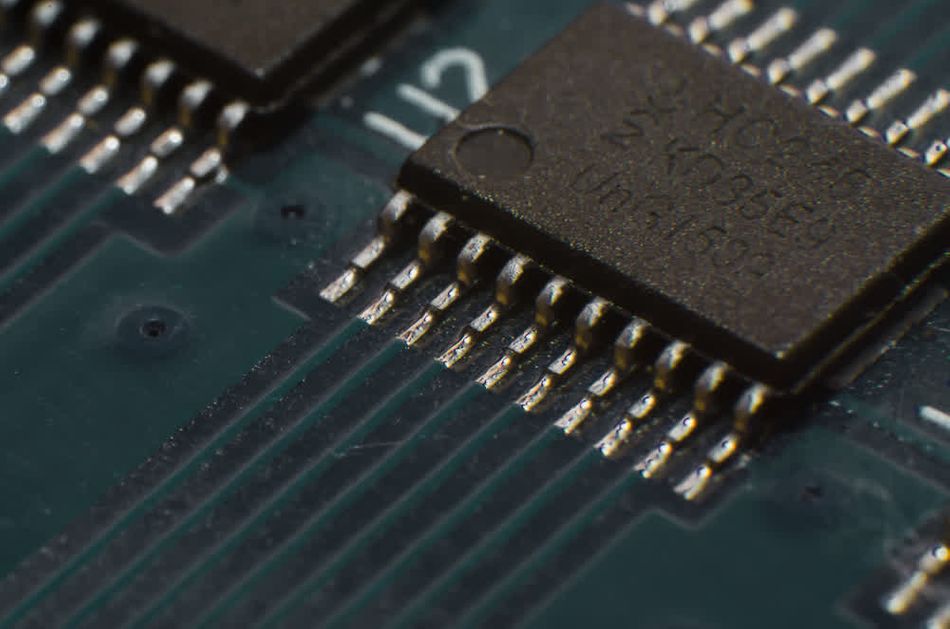
Small Outline Packages: From SOIC to TSOP
Small Outline Integrated Circuit (SOIC) packages represent a significant advancement in surface mount technology, offering a thin, compact alternative to traditional through-hole packages. These packages are characterized by their rectangular shape with gull-wing leads on two sides, allowing for efficient use of PCB real estate and improved electrical performance.
SOIC packages come in various configurations, typically ranging from 8 to 32 pins. The standard SOIC package features include:
Body size: Typically 1.27mm lead pitch
Package height: Ranges from 1.0mm to 2.5mm
Lead pitch: 1.27mm or 0.65mm for narrow versions
Applications: General-purpose ICs, logic devices, and analog circuits
Key features of SOIC packages:
Compact footprint compared to through-hole equivalents
Gull-wing leads for easy soldering and inspection
Available in wide (1.27mm pitch) and narrow (0.65mm pitch) versions
Suitable for automated pick-and-place assembly
Good thermal performance due to large lead surface area
The Thin Small Outline Package (TSOP) is a variation of the SOIC design, offering an even lower profile for applications where vertical space is at a premium. TSOP packages are commonly used in memory devices and have the following characteristics:
Body size: Typically 2.0mm to 3.0mm wide
Package height: Ultra-thin profile ranging from 0.6mm to 1.2mm
Lead pitch: 0.5mm, allowing for higher pin counts in a small area
Applications: Memory chips, DRAMs, Flash memory devices
Key features of TSOP packages:
Extremely low profile for space-constrained designs
Higher pin count capability compared to standard SOIC
Ideal for stacked memory configurations
Enhanced thermal performance due to thinner package
Available in Type I (leads on shorter sides) and Type II (leads on longer sides) configurations
Differences Between TSOP and SOIC
The physical differences between SOIC and TSOP packages are primarily in their dimensions and lead configurations. SOIC packages are generally wider and taller, with a more robust lead structure suitable for a variety of IC types.
TSOP packages, on the other hand, are optimized for thinness and high pin count, making them ideal for memory applications where multiple devices may be stacked.
Suggested Reading: How to Design a PCB Layout: A Comprehensive Guide
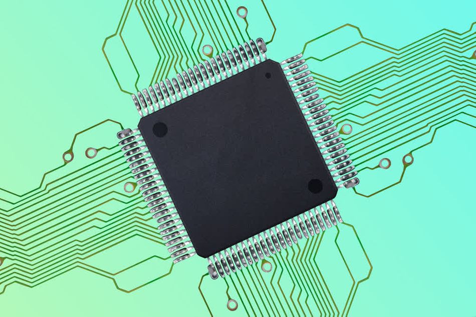
Quad Flat Packages: TQFP, LQFP, and Beyond
Quad Flat Packages (QFP) are a cornerstone of surface mount technology, offering high pin density and versatility in a compact form factor. These packages feature a square or rectangular body with leads extending from all four sides, making them ideal for complex integrated circuits and systems-on-chip (SoC) designs.
The structure of QFP includes:
A flat rectangular body made of plastic or ceramic
Pins arranged in a rectangular grid on the perimeter
Standard lead pitch ranging from 0.5mm to 1.0mm
Electrical connections made through leads to the underlying PCB
This configuration enables high-density circuit designs and facilitates easy connections to various electronic components, contributing to QFP's popularity in modern electronics.
Two prominent variations of QFP are Thin Quad Flat Package (TQFP) and Low-profile Quad Flat Package (LQFP):
TQFP (Thin Quad Flat Package):
Thinner profile, typically around 1.0mm or less
Ideal for applications with limited vertical space
Provides medium heat dissipation capability
LQFP (Low-profile Quad Flat Package):
Lower height compared to standard QFP, but not as thin as TQFP
Suitable for designs requiring very low profile while maintaining thermal management benefits
Often used in automotive and consumer electronics
The choice between TQFP and LQFP depends on specific design constraints related to height and heat requirements.
A comparison of various QFP types, their pin counts, and typical applications:
QFP Type | Pin Count | Typical Applications |
QFP | 16 - 240 | General-purpose ICs |
TQFP | 32 - 144 | Microcontrollers, DSPs |
LQFP | 32 - 256 | Automotive, Consumer electronics |
QFP packages offer several advantages in modern PCB design:
High pin density, accommodating a large number of connections in a compact area
Excellent thermal performance due to their flat structure
Easy surface mounting, designed for automated assembly processes
Ball Grid Array (BGA): High-Density Solutions
Ball Grid Array (BGA) packages represent a significant advancement in high-density integrated circuit packaging technology. BGAs feature a grid of solder balls on the underside of the package, which serve as both electrical connections and mechanical mounting points. This design allows for a much higher pin count in a smaller footprint compared to traditional leaded packages.
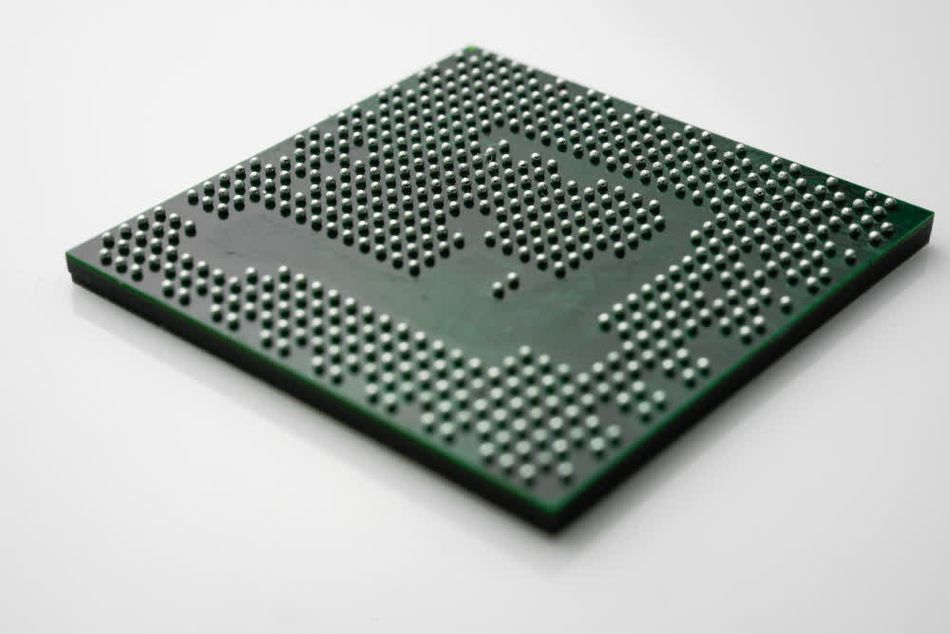
The structure of a BGA package typically includes:
A substrate made of organic material or ceramic
An array of solder balls on the bottom surface
Internal routing layers connecting the die to the solder balls
An encapsulated die attached to the top of the substrate
BGAs offer several advantages:
Higher I/O density in a compact form factor
Improved electrical performance due to shorter interconnects
Better thermal performance through direct contact with the PCB
Self-alignment during reflow soldering process
Reduced parasitic inductance and capacitance
Several BGA variations cater to specific application needs:
FBGA (Fine-pitch Ball Grid Array):
Utilizes smaller ball sizes and tighter pitches
Ideal for mobile devices and other space-constrained applications
TBGA (Tape Ball Grid Array):
Uses a thin, flexible tape substrate
Offers improved thermal performance and reduced package height
CBGA (Ceramic Ball Grid Array):
Features a ceramic substrate for enhanced thermal management
Suitable for high-reliability and high-temperature applications
BGA pitch sizes play a crucial role in PCB design and manufacturability. Common pitch sizes range from 1.0mm down to 0.4mm or even smaller. The choice of pitch impacts several factors:
PCB layer count: Finer pitches often require more PCB layers for routing
Via technology: Smaller pitches may necessitate microvias or buried vias
Recommended Reading: What are Vias in Pad? Advantages, Limitations, Applications, and Comparison with Conventional Vias
Assembly complexity: Tighter pitches demand more precise placement and soldering processes
Inspection requirements: Finer pitches require advanced inspection techniques like X-ray
As technology continues to advance, BGA packages evolve to meet the increasing demands for higher integration, improved performance, and enhanced reliability in electronic systems.
Choosing the Right SMD Package: A Designer's Dilemma
Selecting the appropriate Surface Mount Device (SMD) package is a critical decision in electronic design that significantly impacts the final product's performance, size, and cost. Engineers must carefully weigh several factors to make an informed choice that best suits their specific application requirements.
The following table summarizes the key factors to consider when selecting SMD packages include:
Factor | Decision |
Power Dissipation | Evaluate thermal characteristics and maximum power ratings. |
Signal Integrity | Assess switching speeds and impedance matching needs. |
Board Space | Determine available PCB space and size constraints. |
Thermal Management | Consider heat sink requirements and air flow. |
Cost | Analyze budget limits and packaging costs. |
Application Requirements | Match package type to the intended functionality. |
Real-world examples illustrate the impact of package choice on product performance:
Mobile Devices: The transition from QFP to BGA packages in smartphone processors has enabled higher performance in smaller form factors. BGAs allow for more I/O connections and better heat dissipation, crucial for powerful mobile processors.
Automotive Electronics: LQFP packages are often chosen for automotive microcontrollers due to their robust leads and good thermal performance, essential for the harsh environmental conditions in vehicles.
IoT Sensors: CSP (Chip Scale Package) or WLCSP (Wafer Level Chip Scale Package) are frequently used in IoT devices, allowing for extremely compact designs crucial for wearables and small sensors.
While smaller packages may seem attractive for miniaturization, they can present challenges in assembly and thermal management.
Conversely, larger packages might offer better thermal performance and ease of manufacturing but at the cost of board space.
For instance, choosing between a QFN and a BGA for a high-performance MCU involves trade-offs:
QFN offers simpler PCB design and easier inspection but may limit I/O count.
BGA allows for higher I/O density and potentially better thermal performance but requires more complex PCB design and assembly processes.
SMD Package Trends: Pushing the Boundaries
The evolution of Surface Mount Device (SMD) packaging technology continues to push the boundaries of what's possible in electronic design. Recent advancements are addressing the limitations of traditional packaging methods, enabling the creation of smaller, more powerful, and more efficient electronic devices.
Wafer-Level Packaging
Wafer-level packaging (WLP) integrates ICs at the wafer level, resulting in packages that are nearly the same size as the silicon die itself. WLP offers several advantages:
Ultra-compact form factor, ideal for smartphones and IoT devices
Improved electrical performance due to shorter interconnects
Enhanced thermal characteristics
Potential for cost reduction in high-volume production
3D Packaging
3D Packaging works by stacking multiple ICs vertically, 3D packaging achieves:
Significantly reduced footprint
Improved performance through shorter interconnects
Increased functionality in a single package
Enhanced power efficiency
Embedded Die Technology
This technology incorporates chips directly into the PCB. This approach offers:
Increased circuit density
Reduced interconnect length, improving signal integrity
Better thermal management
Potential for thinner overall device profiles
Fan-Out Wafer-Level Packaging (FOWLP)
This technology addresses the I/O limitations of traditional WLP by redistributing connections in a fan-out design. Benefits include:
Higher I/O count in a compact package
Improved thermal performance
Enhanced electrical characteristics
Flexibility in chip connection schemes
Multi-Chip Modules
Multi-Chip Modules (MCMs) combine multiple chips in a single package, offering:
Improved system integration
Reduced overall footprint
Enhanced performance through optimized chip-to-chip communication
Potential for cost reduction in complex systems
These advanced packaging technologies are addressing several key limitations in electronics design:
Size constraints: Enabling further miniaturization of electronic devices
Performance bottlenecks: Improving signal integrity and reducing latency
Thermal management: Enhancing heat dissipation in high-performance applications
Integration challenges: Allowing for more complex systems in smaller form factors
Cost considerations: Potentially reducing overall system costs through higher integration
The following table compares traditional SMD packages with cutting-edge alternatives:
Aspect | Traditional Package (e.g., BGA) | Cutting-Edge Package (e.g., FOWLP) |
Pin Count Range | 16 - 256 | Hundreds |
Package Size | Very compact | Ultra-compact |
Thermal Performance | Excellent | Excellent |
Key Use Case | High-performance ICs | Wearables, Smartphones |
Integration Level | Single chip | Multiple chips or system-level |
Interconnect Length | Longer | Significantly shorter |
Manufacturing Complexity | Moderate | High |
Cost (high volume) | Moderate | Potentially lower |
Thermal Management for SMD Packages
Effective thermal management is crucial for the reliability and performance of Surface Mount Device (SMD) based circuits. As electronic devices become more compact and powerful, managing heat dissipation becomes increasingly challenging.
Different SMD package types present unique thermal challenges:
Quad Flat Packages (QFP): Heat dissipation primarily occurs through the leads and top surface, which can be limiting for high-power applications.
Ball Grid Arrays (BGA): While offering better thermal performance than QFPs due to their larger contact area with the PCB, they can still struggle with heat dissipation in high-density designs.
Chip Scale Packages (CSP): Their ultra-compact size makes heat dissipation particularly challenging, often requiring advanced thermal management techniques.
Power Packages (e.g., D2PAK, TO-263): These are designed for high power dissipation but still require careful thermal design, especially in compact layouts.
Various thermal management techniques can be employed to address these challenges:
Thermal Vias: These are plated through-holes that conduct heat from the top layer to inner or bottom layers of the PCB, effectively increasing the heat dissipation area.
Heat Spreaders: Metal plates or structures that distribute heat over a larger area, improving overall thermal performance.
Thermal Interface Materials (TIMs): These materials improve thermal conductivity between the package and heat sink or PCB.
Active Cooling: For high-power applications, fans or liquid cooling systems may be necessary to maintain safe operating temperatures.
PCB Layout Optimization: Proper component placement and copper pour design can significantly improve heat dissipation.
Calculating thermal performance is essential for effective design. The key formula for estimating junction temperature is:
Tj = Ta + (P * R_theta)
Where:
Tj is the junction temperature (°C)
Ta is the ambient temperature (°C)
P is the power dissipation (W)
R_theta is the thermal resistance (°C/W)
For example, with a power dissipation of 1W, thermal resistance of 50°C/W, and ambient temperature of 25°C:
Tj = 25 + (1 * 50) = 75°C
This calculation helps engineers determine if the junction temperature remains within the component's specified limits.
Best Practices for Thermal Management
Best practices for thermal design in SMD-based circuits include:
Conduct thorough thermal analysis during the design phase
Use thermal simulation tools to identify hotspots and optimize layouts
Implement sufficient copper pour areas for heat spreading
Consider the use of high thermal conductivity PCB materials for critical applications
Ensure adequate spacing between heat-generating components
Utilize thermal vias effectively, especially for BGA packages
Choose appropriate thermal interface materials for heat sinks or cooling solutions
Implement proper airflow design in enclosures
Monitor temperature-sensitive components during prototype testing
Consider derating components for improved long-term reliability
Conclusion
Surface Mount Device (SMD) package types and sizes play a crucial role in modern electronic design. The diverse range of packages, from chip components to complex integrated circuits, offers engineers flexibility in designing compact and efficient electronic systems. Understanding the characteristics of different SMD packages, such as QFP, BGA, and SOT, is essential for optimizing board space, thermal management, and overall performance.
The ongoing miniaturization trend in electronics continues to drive innovations in SMD packaging, with advancements like wafer-level packaging and 3D IC integration pushing the boundaries of what's possible. These developments are enabling the creation of smaller, more powerful devices across various industries, from consumer electronics to automotive and medical applications.
Frequently Asked Questions
What is the difference between SMD and SMT?
SMD (Surface Mount Device) refers to the electronic components designed for surface mounting, while SMT (Surface Mount Technology) is the method used to mount these components onto printed circuit boards.
How do I choose the right SMD package for my design?
Consider factors such as power requirements, thermal management, available board space, signal integrity needs, and manufacturing capabilities. Balance these factors against the specific requirements of your application to select the most appropriate package.
What are the advantages of using smaller SMD packages?
Smaller packages allow for higher component density, reduced board size, potentially lower costs, and improved electrical performance due to shorter signal paths. However, they may present challenges in terms of assembly and thermal management.
How does the choice of SMD package affect thermal management?
Package size and design significantly impact heat dissipation. Larger packages generally offer better thermal performance, while smaller packages may require additional thermal management techniques such as thermal vias or heat spreaders.
What are the key considerations when working with BGA packages?
BGA packages offer high I/O density but require careful PCB design considerations, including layer stack up, via strategy, and routing complexity. They also necessitate specialized equipment for assembly and inspection.
How do I interpret SMD package codes (e.g., 0402, 0603)?
These codes typically represent the package dimensions in hundredths of inches. For example, 0402 indicates a package size of 0.04" x 0.02" (1.0mm x 0.5mm).
What emerging SMD package technologies should I be aware of?
Keep an eye on advancements in wafer-level packaging (WLP), fan-out wafer-level packaging (FOWLP), 3D packaging, and embedded die technology. These innovations are driving further miniaturization and improved performance in electronic designs.
References
in this article
1. Introduction2. The SMD Revolution: Shrinking Electronics3. Decoding SMD Package Nomenclature4. SMD Package Types and Form Factors Chip Components: Resistors and Capacitors5. Small Outline Packages: From SOIC to TSOP6. Choosing the Right SMD Package: A Designer's Dilemma7. SMD Package Trends: Pushing the Boundaries8. Thermal Management for SMD Packages9. Conclusion10. Frequently Asked Questions11. ReferencesNo time now? Save for later.
We only use your email to send this link. Privacy Policy.