Trace Width vs Current in PCB Design
This article explores the key factors influencing trace width, provides practical guidelines, and highlights best practices for selecting the correct dimensions based on current-carrying demands in modern PCB design.

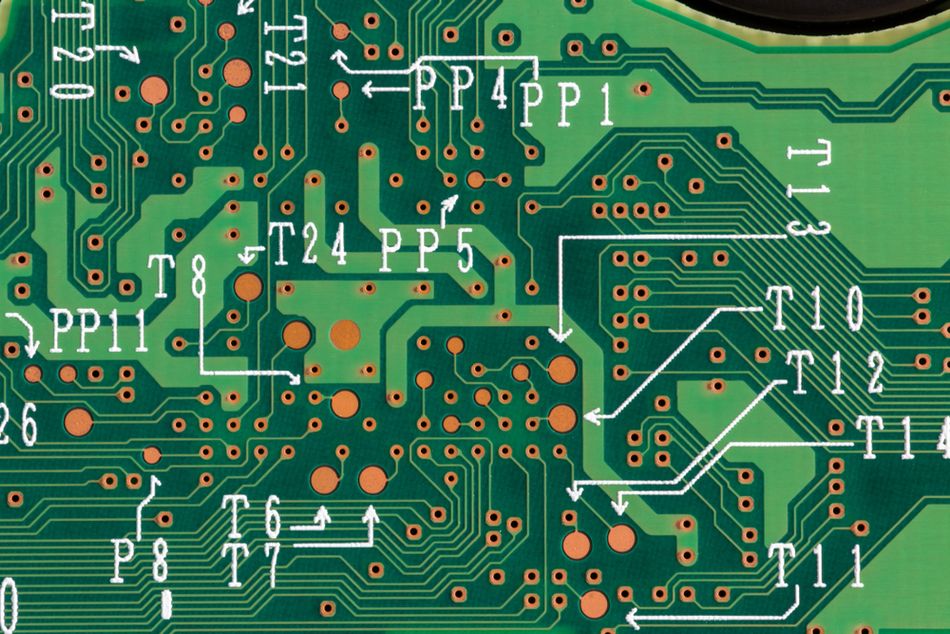
Traces on a Printed Circuit Board (PCB)
Introduction
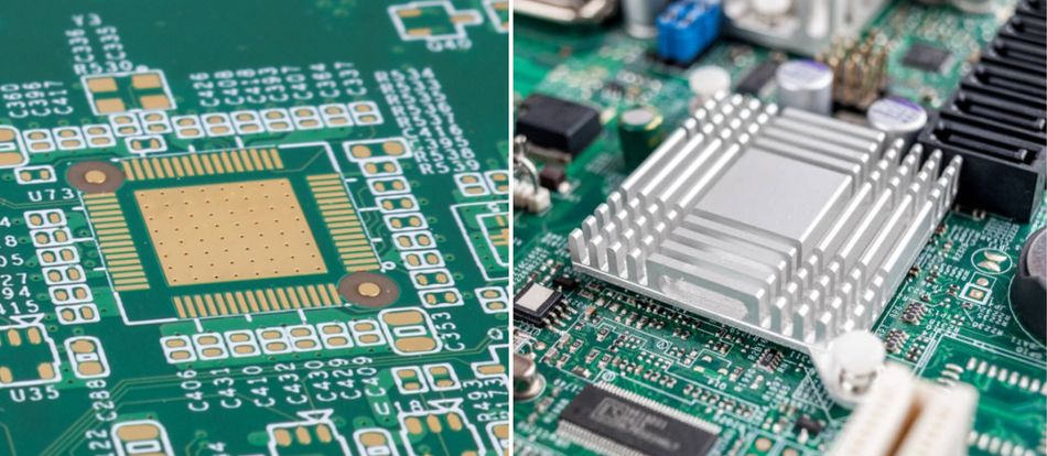
PCB trace width refers to the physical width of the copper pathways on a printed circuit board that carries electrical current. It is an essential design parameter because trace width directly impacts how much current a trace can safely carry without overheating or failing. If a trace is too narrow for the current flowing through it, the higher electrical resistance of the trace will cause excessive Joule Heating (I²R losses), leading to heat buildup. This can result in voltage drops, reduced efficiency, or even burnt traces and board damage in extreme cases. Conversely, making traces wider than necessary can waste valuable PCB space and complicate the layout.
Current capacity is, therefore, a crucial factor in PCB design! Each trace must be sized to handle the expected current load under its operating conditions (e.g. ambient temperature, copper thickness, allowable temperature rise) without creating hot spots or reliability issues. Much like choosing the right wire gauge for a given current, PCB designers must choose appropriate trace widths for power and ground lines, high-current paths, and even signal lines that carry significant current.
In this article, we will discuss the ways to determine the optimal trace width vs current for various applications, including high-current and sensitive signal traces. By mastering the principles of trace width vs current, designers can ensure robust and efficient PCB layouts!
Theoretical Background
Trace Width, Resistance, and Current Carrying Capacity
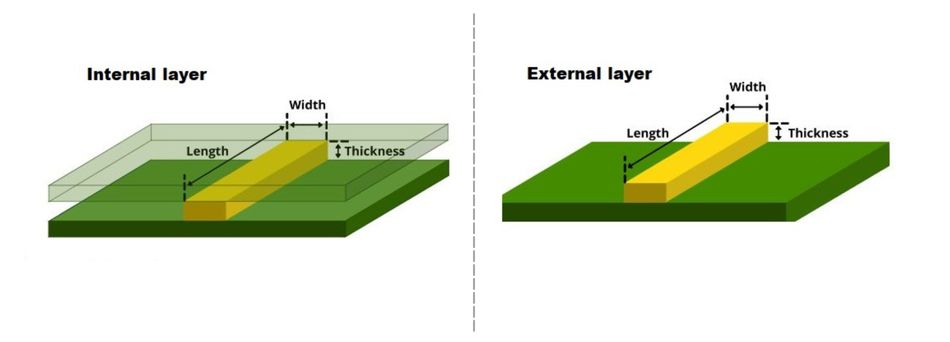
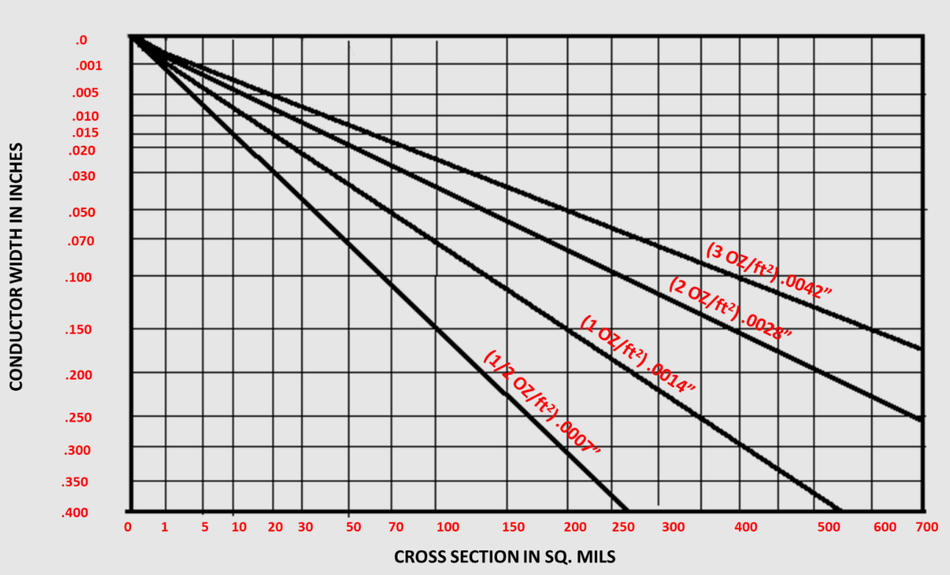
In PCB design, the trace width vs current relationship is governed by fundamental electrical principles, particularly Ohm’s Law and Joule’s Law. There is a direct relationship between the cross-sectional area of a trace and the current it can carry safely. The cross-sectional area is determined by the trace width and the copper thickness (height) of the trace. A larger cross-sectional area (wider and/or thicker trace) has lower electrical resistance, which means less heat is generated for a given current flow.

where P is the power dissipation, I is the current, and R is the resistance
This implies that a narrower trace, having higher resistance, will dissipate more heat than a wider one carrying the same current. This is why widening a trace reduces its temperature rise – the current is distributed over a greater area, lowering the resistance and thus the I²R losses. [1]
The electrical resistance of a copper trace is given by the equation:

where ρ is copper’s resistivity, L is the trace length, W is the trace width, and T is the trace thickness (which depends on copper weight)
From this relation, for a fixed length and copper thickness, a wider trace (larger W) yields a lower resistance. Lower resistance not only reduces heat, but also minimizes voltage drop along the trace (important for power delivery lines). [2]
Recommended Reading: PCB Trace: The Backbone of Modern Circuit Design
Heat Dissipation and Thermal Considerations
In PCB design, managing heat dissipation is critical when analyzing trace width vs current performance. As the current flows through a PCB trace, the resistive heating causes the trace temperature to rise above ambient. The trace will reach an equilibrium temperature where the heat generated (I²R) is equal to the heat dissipated into the environment (through conduction into the PCB laminate and copper planes, and convection/radiation to the air if it’s an outer layer).
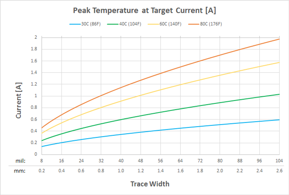
If the trace generates more heat than can be dissipated, its temperature will keep rising, potentially damaging the PCB (burnt or delaminated traces) or affecting nearby components. Designers, therefore, specify an allowable temperature rise (ΔT) for traces, often in the range of 10°C to 30°C above ambient, to ensure reliability. [3]
Heat dissipation depends on whether the trace is on an external layer (exposed to air) or an internal layer (embedded in the PCB). External traces can dissipate heat more easily into the surrounding air, whereas internal traces are surrounded by insulating laminate, so heat removal is slower. Traditional standards assumed that internal traces carry less current than external ones for the same width due to this difference in cooling. However, modern studies (IPC-2152) have shown that with proper thermal management (e.g. copper planes conducting heat), internal traces can handle nearly as much current as external ones for a given cross-sectional area.
Designers must balance current needs with acceptable temperature rise and ensure adequate cooling or heat spreading for high-current traces. As a rule of thumb, shorter traces also help thermal performance – a long high-current trace will have more total I²R loss (and temperature rise) than a short one.
IPC-2221 vs IPC-2152: Standards for Trace Width Calculations
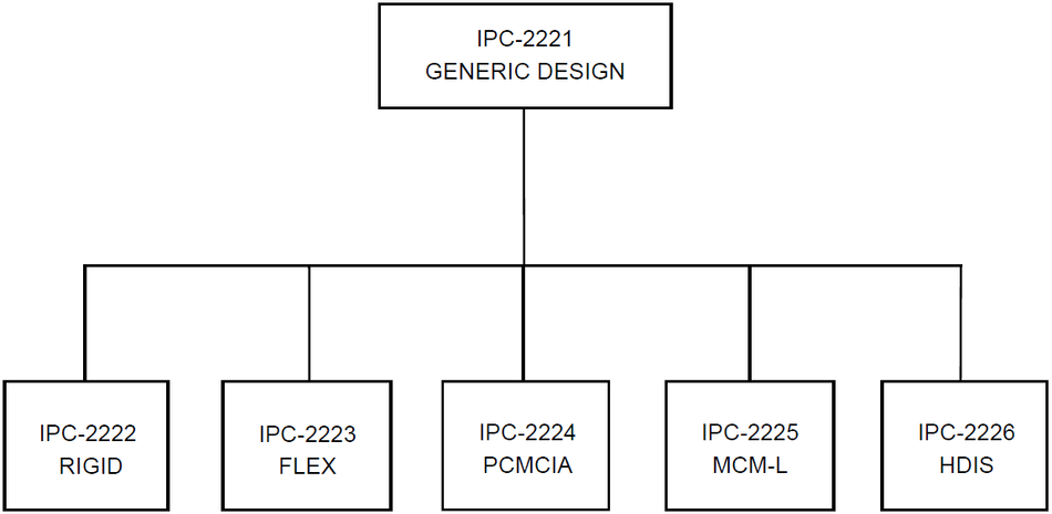
To help engineers determine the appropriate trace width for a given current and temperature rise, industry standards provide guidelines and empirically derived formulas. IPC-2221 (a generic PCB design standard) included classic charts and a formula for trace current capacity based on testing done decades ago.

where I is the current in amperes, ΔT is the permitted temperature rise in °C, and A is the cross-sectional area of the trace in square mils (width × thickness). The constant k depends on whether the trace is on an external layer or internal layer (approximately 0.048 for external and 0.024 for internal). This formula captures the idea that a larger area trace (A) can carry more current, and that allowing a larger temperature rise (ΔT) also increases current capacity.
However, IPC-2221 is limited by its testing scope—it was derived from controlled conditions (single copper weight, specific board setup, still air) and doesn't consider modern design variables such as board stack-up, copper planes, or forced airflow. By the 2000s, the electronics industry recognized the need for updated guidance.
Notably, IPC-2152 incorporates factors such as: copper weight (thickness), whether the trace is external or internal, and even the external cooling environment (air vs vacuum) in determining current carrying capacity. It was found that internal traces, when embedded in a board with good thermal conductivity or adjacent planes, can carry nearly as much current as external ones – a revision of the older guideline that always derated internal traces heavily.
Overall, IPC-2152 gives more accurate results and often allows slightly smaller trace widths than IPC-2221 for the same current, because it accounts for modern PCB practices (like using copper pours or planes to spread heat). Today, designers use IPC-2152 charts or calculators based on them for sizing high-current traces, while the formula for IPC-2221 is considered conservative but still used for quick estimates or when in doubt.
Recommended Reading: IPC Class System: A Technical Deep Dive into Patent Classification Architecture
Practical Considerations in Selecting Trace Width
Selecting the proper trace width in a PCB design involves applying the above theory and standards to real-world design constraints. Here are key practical considerations:
1. Industry Guidelines and Default Rules:
Many PCB design tools and fab houses have default trace width standards (for example, 6 or 10 mils for signal traces). However, these defaults are for ordinary low-current signals and are not always suitable for power traces. For power delivery and high-current paths, designers should refer to current capacity tables or calculators. A common guideline is “1 mm of trace width per ampere” as a rough rule of thumb for 1 oz copper, external layer, with moderate temperature rise, but this is very approximate. A more accurate approach is to use IPC-2152/2221 data.
The table below shows example recommended trace widths for different currents on an external 1 oz copper trace, for a 10°C temperature rise (based on IPC standards):
| Current (A) | Trace Width (mil) | Trace Width (mm) |
| 0.5 | ~6 | ~0.15 |
| 1 | 10 | 0.25 |
| 2 | 30 | 0.76 |
| 3 | 50 | 1.27 |
| 4 | 80 | 2.03 |
| 5 | 110 | 2.79 |
| 7 | 180 | 4.57 |
| 10 | 300 | 7.62 |
These values apply to outer-layer traces in air with 1 oz copper and a 10°C temperature rise. As temperature rise tolerance increases (e.g., 20°C), the required trace width decreases by roughly 25–30%. Conversely, for heat-sensitive designs requiring minimal ΔT, wider traces or enhanced cooling are necessary.
2. Copper Thickness (Weight):
Copper weight, typically measured in ounces per square foot, directly affects the current-carrying capability of a trace. Common values include 1 oz (≈35 µm), 2 oz, and 3 oz. Thicker copper increases the cross-sectional area of the trace, lowering resistance and allowing higher current for the same width. Doubling copper thickness can improve current capacity by 60 – 100% for a given ΔT. For example, a 1 mm wide, 2 oz copper trace can safely carry ~4.2 A with a 10°C rise, compared to ~2–2.5 A for the same trace at 1 oz. Designers must specify copper weight per layer in fabrication notes. Additionally, plating on outer layers can increase effective copper thickness slightly, enhancing capacity.
3. Trace Placement: External vs Internal Layers
The external (outer layer) traces dissipate heat more readily, so they traditionally were allowed to carry more current than internal traces. IPC-2152 provides separate charts/nomographs for internal and external traces. In practice, if you have a very high current net, you might route it on an outer layer to help cooling, or use thermal vias to connect an inner-layer trace to copper pours or heatsinks.
4. Length of the Trace
While the current rating of a trace is usually given per unit length (assuming a uniform section), an extremely long trace will drop more voltage and distribute heat along its length. Long high-current traces can act like resistive heaters. The goal should be to keep high-current paths as short and direct as possible. If the routing requires a longer path, consider using a wider trace or splitting the current into multiple paths to reduce the I²R losses in each segment.
5. PCB Layer Stacking and Vias:
Multilayer boards often use vias to transfer current between layers. However, vias have a limited current-carrying capacity—typically around 0.5 A per via. High-current paths must use multiple vias in parallel (via stitching) to prevent overheating. For example, a 5 A net may require 5–10 vias in an array. For extremely high currents, alternatives like press-fit pins or busbars may be used. Designers can also distribute current across multiple layers using wide traces or power planes, interconnected with stitched vias to evenly share the load—especially valuable when space is constrained.
6. Design Safety Margins
It’s good practice to add some safety margin to trace width beyond the bare minimum calculated. Small variations in manufacturing (trace etching tolerance), unexpected rises in ambient temperature, or additional heating from neighboring components could all push a trace closer to its limit. Many engineers oversize power traces a bit “just in case.” For instance, if the calculator says 15 mil is enough, you might use 20 mil if space allows. The repetitive surge currents (spikes) or inrush currents (e.g. charging a capacitor bank) might momentarily exceed the steady-state current – a thicker trace can handle short surges better by absorbing heat capacitively in the thermal mass of copper.
Selecting appropriate trace width vs current is a multidimensional design decision involving thermal, mechanical, and electrical trade-offs. By considering copper thickness, trace placement, via strategy, and safety margins, engineers can ensure robust and reliable PCB performance under varying operational conditions.
Recommended Reading: PCB Via: Essential Guide to Vertical Interconnect Access in Circuit Boards
Calculation Methods and Formulas
Determining the appropriate trace width vs current in PCB design involves applying empirical standards, equations, and design tools. Engineers use a combination of IPC guidelines, formula-based estimations, and software calculators to ensure their traces are sized correctly for the expected current and temperature rise. Below are their details:
1. IPC-2152 Nomographs and Charts
The IPC-2152 standard includes published curves (nomographs) that allow you to look up the required cross-sectional area of a trace for a desired current and temperature rise. The procedure typically is: choose your acceptable temperature rise (e.g. 10°C or 20°C), identify if the trace is internal or external, then use the chart to find the trace cross-sectional area needed for your target current (amps). After that, you convert the cross-sectional area to a specific width, given your copper thickness. This method is reliable and accounts for many factors, but it can be a bit cumbersome to do manually. In practice, many have digitized these charts into calculators.
2. Empirical Formula (IPC-2221)
For quick calculations, the IPC-2221 standard offers a simplified empirical formula based on earlier testing:

where, I is the current in (Amperes), ΔT is the Temperature rise (°C), A is the cross-sectional area (mil²), and k is the constant: 0.048 for external layers, 0.024 for internal layers
The formula is rearranged to solve for the area:

To calculate trace width in mils:

Where t(oz) is the copper thickness in ounces per square foot (1 oz ≈ 1.378 mils thick)
Example: To carry 5 A on an external 1 oz copper layer with a 10°C temperature rise:


This result aligns with the conservative guidelines of IPC-2221. If the allowed ΔT is increased to 20°C, the required width drops significantly (~70 mil), illustrating how trace width is highly sensitive to thermal limits.
3. Online Calculators and Tools
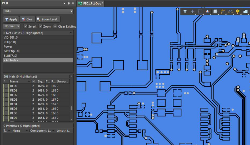
Numerous online tools—offered by manufacturers like AdvancedPCB, Altium, and Digi-Key —incorporate IPC-2152 or IPC-2221 logic. These calculators allow users to input current, copper weight, temperature rise, and layer type to instantly compute the minimum trace width. Most modern CAD tools (e.g., KiCad, Altium, Cadence) also include trace width calculators or rule-checking features that validate trace current capacity during layout. [5] It is better to verify which IPC standard the calculator uses—IPC-2221 is more conservative, while IPC-2152 is based on newer data and may yield narrower (but still safe) results.
Example Calculations: Let’s consider a couple of design scenarios:
1. PCB Power Rail: You have a PCB with a 5 V power rail that will carry up to 4 A to various loads. The board uses 1 oz copper. If we target a 20°C temperature rise, a calculator (using IPC-2221) might suggest ~50–60 mil (≈1.5 mm) width on an external layer for that 4 A. If that trace had to go through an internal layer, we might widen it by ~2× or more (or use 2 oz copper on that layer) to compensate. To be safe, an engineer might choose 80 mil for a margin. If space is tight, alternatively they could use a 40 mil trace but on 2 oz copper to achieve a similar effect.
2. High Current Motor Driver: A design drives a 10 A motor from a MOSFET on the PCB. This is a high current, and 10 A with 1 oz copper (10°C rise) requires roughly 300 mil (7.6 mm) width if using just a normal trace. If the board cannot accommodate a 7.6 mm wide trace, solutions could include: using 2 oz copper (which cuts the required width nearly in half for the same ΔT), routing the current through two 4 mm wide traces in parallel on different layers (each carrying ~5 A) with plenty of via connections between them, or soldering a bus bar or thick wire onto the PCB to handle the current. In practice, power electronics boards often use copper weights of 2–3 oz and combine multiple strategies to manage such currents.
4. Using Simulation
For critical designs, some engineers use thermal simulation tools (e.g., ANSYS, SolidWorks PCB, or built-in solvers of the Altium Designer) to model the PCB and verify that the chosen trace widths will keep temperatures in check.
Recommended Reading: Microvias: Pioneering the Future of PCB Design and Electronics Miniaturization
Common Mistakes and Troubleshooting
Designing with the correct trace width vs current relationship is essential for PCB reliability, but practical missteps can lead to overheating, failures, or degraded performance. Below are common mistakes engineers make—and how to troubleshoot or avoid them.
1. Using Undersized Traces
A frequent mistake is relying on default EDA tool trace widths (like 10 mil) for all connections, including power rails. An undersized trace will overheat under high current, leading to discoloration or burnt PCB areas, intermittent circuit behavior, or complete trace failure (the copper can delaminate or even vaporize like a fuse if severely overloaded).
Troubleshooting Tip: If a board resets or a regulator drops out under load, measure voltage across the trace. A noticeable drop suggests excessive resistance. Always oversize power traces based on the actual current draw—not default settings.
2. Ignoring Copper Weight and Plating
Designing with a specific copper weight (e.g., 2 oz) but manufacturing with a different one (e.g., 1 oz) can halve the effective cross-section, causing unexpected heating. Outer-layer plating also affects thickness—use fabrication notes to specify copper weight clearly. For mixed needs (fine pitch and heavy current), advanced techniques like selective plating or copper coin inserts may be needed.
Troubleshooting Tip: If traces overheat unexpectedly, verify the actual copper weight used—cross-sectioning or resistance measurements can help identify discrepancies.
3. Not Using Enough Vias for High Current Transfers
Relying on a single via to connect large copper pours across layers creates a bottleneck. A typical via can handle ~0.5 A; higher currents require via stitching or larger/high-current vias. Inadequate vias can lead to trace failure even if the surface copper is wide enough.
Best Practice: Use multiple vias (via stitching) for any high-current path between layers. For 10 A, at least 20 small vias or fewer large, filled vias should be used. Solder-filled or copper-filled vias increase reliability in power applications.
4. Sharp Corners and Neck-Downs
Sudden track width reductions or 90° bends cause localized current crowding, increasing heat and inductance. These narrow or sharp sections are common failure points, especially at connector pins or tight routing areas.
Troubleshooting Tip: If you suspect a certain corner of a trace is getting hotter, an IR thermal camera or even carefully touching (with appropriate safety) can sometimes find the hot spot. Use 45° bends or rounded corners for smoother current flow. If neck-downs are necessary, keep them short and consider parallel traces or extra pins for current sharing.
5. Overlooking Thermal Relief for Heat Dissipation:
Thermal reliefs (spoked connections between pads and planes) ease soldering but limit current capacity. Applying them to high-current pins restricts copper cross-section, creating hotspots or soldering failures.
Solution: Avoid thermal reliefs on high-current pads. Use solid copper connections and compensate with selective soldering techniques or preheating to ensure reliable joints.
6. Lack of Thermal Management
High-current traces not only heat themselves but also warm nearby components. Placing multiple high-power traces or devices in close proximity without thermal planning causes localized hotspots.
Best Practice: Use copper pours, thermal vias, and heatsinks to spread heat. Separate high-current traces across layers or provide airflow and spacing to minimize heat stacking.
7. EMI/Signal Integrity Issues:
High-current traces can introduce electromagnetic interference (EMI), especially if routed near sensitive analog or high-impedance signals. This results in circuit instability, especially in mixed-signal designs.
Troubleshooting Tip: Observe noise-related symptoms (e.g., buzzing in audio lines when motors run) and reroute sensitive traces away from power lines. Use orthogonal routing between layers and introduce shielding or snubbers if needed.
Recommended Reading: PCB Design: A Comprehensive Guide to Printed Circuit Board Design
Conclusion
The relationship between trace width and current is a critical aspect of PCB design that directly impacts the safety, reliability, and performance of electronic systems. Wider and thicker traces allow higher current flow by minimizing resistance and heat buildup, while undersized traces risk thermal damage and failure. IPC-2152 and similar standards offer a reliable framework for trace sizing, and practical strategies—such as increasing copper weight, using parallel paths, and proper via placement—enhance power handling.
Modern PCB design is evolving, with new materials, thermal management techniques, and intelligent design tools making it easier to optimize power delivery. Yet, the core principles remain unchanged: always size traces based on real-world current requirements, include safety margins, and consider the entire thermal and electrical environment. With careful planning and compliance with the best practices, engineers can design robust PCBs that withstand demanding applications and ensure long-term performance and reliability.
Frequently Asked Questions (FAQs)
Q: How do I determine the right PCB trace width for a specific current?
A: Use a PCB trace width calculator based on IPC-2152 or IPC-2221. Input your operating temperature, copper weight, and current. This tool minimizes power loss and helps ensure trace reliability. It's essential in PCB manufacturing to specify trace width precisely, especially for high-current PCB assembly applications.
Q: What’s the difference between IPC-2221 and IPC-2152 for trace current capacity?
A: IPC-2221 uses a conservative formula; IPC-2152 offers updated, realistic sizing using modern cooling and materials. IPC-2152 better reflects real PCB manufacturing conditions, allowing slightly smaller widths. Use IPC-2152 when accuracy matters—especially in high-frequency or dense PCB assembly designs requiring precise thermal control.
Q: How does copper thickness (1 oz vs 2 oz etc.) affect current carrying capacity?
A: Thicker copper reduces trace resistance, supporting higher maximum current and reducing power loss. For instance, 2 oz copper can carry ~60–80% more current than 1 oz. Always specify copper weight during PCB manufacturing to ensure the trace performs within safe operating temperature limits.
Q: What happens if a PCB trace is too narrow for the current?
A: Too-narrow traces lead to overheating, increased trace resistance, and eventual failure. Symptoms include excessive power loss, voltage drop, and potential delamination. During PCB assembly, these issues compromise reliability. Proper width sizing using a PCB trace width calculator prevents failures and ensures thermal stability.
Q: Can I use multiple smaller traces or layers in parallel to handle a high current?
A: Yes, parallel traces on different layers reduce trace resistance and help with thermal management. Use sufficient vias for current distribution. This method is helpful in space-constrained designs and high-power pcb manufacturing scenarios. Ensure similar lengths and widths to balance the load across traces effectively.
Q: Do I need wider traces for inner layers compared to outer layers for the same current?
A: Inner layers have limited cooling and higher operating temperature. IPC-2152 shows less drastic derating than IPC-2221, but inner traces may still need extra width. Use thermal vias or adjacent copper planes. Conservative designs oversize internal traces to avoid overheating, especially near the maximum current threshold.
References
[1] Cadence. Joule's Law of Electric Heating [Cited 2025 March 25] Available at: Link
[2] Research Gate. Thermal Design Guideline of PCB Traces under DC and AC Current [Cited 2025 March 25] Available at: Link
[3] MCL PCB. What is the Maximum Temperature for PCBs? [Cited 2025 March 25] Available at: Link
[4] IPC International. IPC-2152 - Standard for Determining Current Carrying Capacity in Printed Board Design [Cited 2025 March 25] Available at: Link
[5] Altium. Using an IPC-2152 Calculator: Designing to Standards [Cited 2025 March 25] Available at: Link

