Advancing Flexible Electronics: Printing Multilayer Membrane Keyboards with Conductive Inks
Flexible membrane keyboards are used in a variety of electronics, medical devices, automotive, and more due to their thin, lightweight design. This project demonstrates printing one using Voltera’s NOVA system.
18 Feb, 2025. 4 minutes read
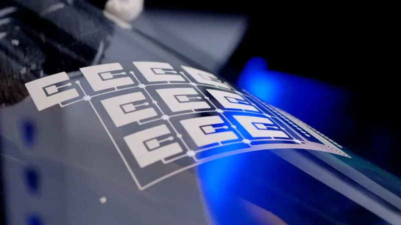
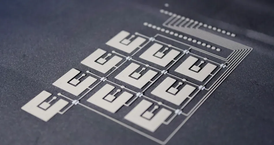
Figure 1: Three layered print with crossovers
This article was first published on
www.voltera.ioAs demand for thinner, more adaptable electronics grows, advanced manufacturing techniques like printed electronics are enabling new possibilities. Flexible membrane keyboards are essential in industries ranging from consumer electronics to aerospace, offering a lightweight and durable alternative to traditional input devices. This article explores how Voltera’s NOVA materials dispensing system can be used to print a fully functional multilayer flexible membrane keyboard, leveraging conductive and dielectric inks for high-performance circuitry.
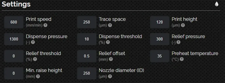
Project overviewThe purpose of this project is to demonstrate how NOVA prints multilayer electrical circuits on a highly flexible substrate (PET), and dispenses ink with high precision on sections that are as small as 250 µm W × 40 µm H. |
Design layout
We divided the layout into three layers:
- Base conductive layer (ACI SS1109 Stretchable Silver Ink)
- Dielectric layer (ACI SI3104 Stretchable Printed Insulator)
- Top conductive layer (ACI SS1109 Stretchable Silver Ink)
Desired outcome
Based on a matrix style keyboard design, we limited the number of pins used to only seven on the controller (Arduino Micro, A000053). Once connected to a power source, pressing any key on the keyboard will trigger the controller to register the key.
Functionality
We determined a 10-numbered keypad design would be suitable for this project. However, other flexible membrane keyboard designs have the potential for further customization, such as specific graphics, colors, or lighting, which could be beneficial for specialized equipment, including customized control panels, wearable devices, and foldable electronics.
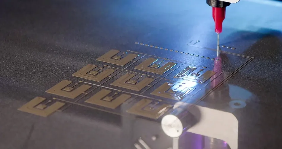
Printing and curing the flexible substrate
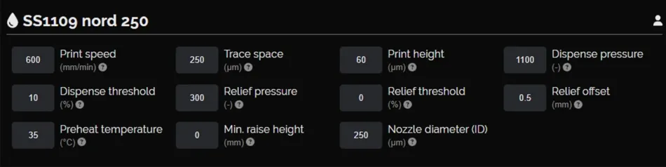
Base conductive layer
This layer consists of a 4’’ × 3’’ matrix grid for 10 numbered keys, excluding the 10 dielectric pads (see dielectric layer).

| Ink | ACI SS1109 stretchable silver ink |
| Substrate | PET |
| Nozzle type | Nordson EFD 7018333 dispensing tip, 0.25 mm inner diameter |
| Probe pitch | 5 mm |
| Cure time and temperature | 5 minutes at 135°C |
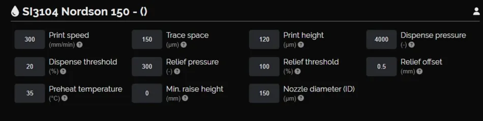
Dielectric layer
This layer consists of 10 dielectric pads. To ensure full coverage of the dielectric ink, we did two passes for this layer, each cured after dispensing.


| Ink | ACI SI3104 stretchable printed insulator |
| Substrate | PET |
| Nozzle type | Nordson EFD 7018424 dispensing tip, 0.15 mm inner diameter |
| Probe pitch | 2 mm |
| Cure time and temperature | 5 minutes at 135°C |
Top conductive layer
This layer consists of 10 fine crossover lines that connect the red signal paths and complete the circuitry.

| Ink | ACI SS1109 stretchable silver ink |
| Substrate | PET |
| Nozzle type | Nordson EFD 7018333 dispensing tip, 0.25 mm inner diameter |
| Probe pitch | 2 mm |
| Cure time and temperature | 5 minutes at 135°C |
Challenges and advice for printing multilayer
Broken layers
Because inks from different manufacturers have different properties – they may contain solvents that dissolve existing traces for example – printing and curing each new layer risks breaking the layer previously completed. It is, therefore, crucial that you choose compatible materials based on the degree of flexibility required.
For this project, we selected compatible inks from ACI Materials, but for projects that involve using multiple inks from different manufacturers, it is recommended that you check the materials’ technical data sheets.
Electrical shorts
Due to the matrix design of the keyboard, the signal lines have a number of crossovers, which could cause electrical shorts if not insulated properly.
Printing a second pass of the dielectric layer achieves an appropriately thick insulating layer and supports further printing on top.
Connection issues
Because the crossover sections are intricate (250 µm W × 40 µm H), if the nozzle scratches the ink while printing, the electrical paths may not function as planned.
Separating the crossover sections into their own layer (the top conductive layer) allows each crossover pad to be probed accurately and have specialized settings, yielding a higher success rate.
In addition, because changes in height can happen drastically when printing over existing traces, setting a low probe pitch will make the height map more accurate. An accurate height map means the height transition at the edges of features is accurate and the risk of traces being printed off-course is low.
Post-printing: A fully flexible electronic device
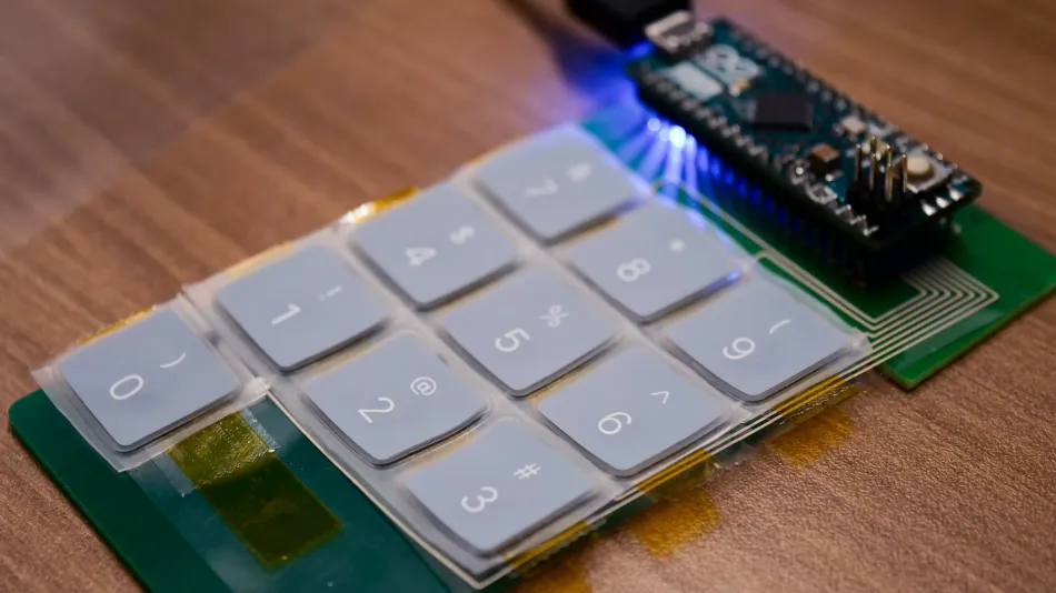
To ensure the Arduino Micro was securely in place, we used a FR1 board, cut it to 30 mm × 60 mm, and placed it beneath the flexible substrate (PET sheet). Next we drilled through holes on the board and the flexible substrate with the Voltera V-One PCB printer.
We then dispensed solder paste, placed the diodes on the flexible substrate, and riveted it together with the FR1 board, before placing the metal switches on the rectangle-shaped contacts. To secure the metal switches, we covered them with Kapton tape.
Next, we secured the controller to the flexible substrate and connected it to a power source. We also gave the keyboard a finishing touch by placing it inside a 3D-printed enclosure with graphical silicone keys.

Conclusion
This project highlights the innovative potential of printing on flexible substrates. It also points to the critical role of fine-tuning print settings to achieve success in multilayer projects.
As achieved by this project, using compatible materials helps ensure optimal performance, and is key to unlocking the full potential of flexible electronics. As we continue to explore the boundaries of what’s possible with flexible substrates, we invite you to view the other projects we’ve completed.