Aluminum PCB Design: Advanced Thermal Management Solutions for High-Power Electronics
This technical guide examines aluminum PCB architecture, manufacturing processes, thermal characteristics, and implementation methodologies for optimal thermal performance in high-power electronic systems.
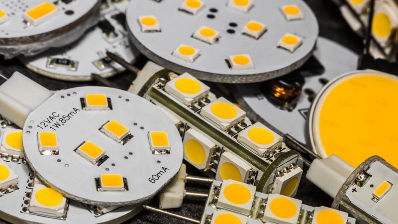
Aluminium PCBs - G4 LED bulbs in different Sizes, and Shapes
Introduction
Thermal management has become a critical challenge in modern electronics, with devices generating heat loads exceeding 500 W/cm². Electronic component failures due to thermal stress account for 55% of all hardware malfunctions, while inadequate heat dissipation reduces operational lifespan by up to 40%. Traditional FR-4 PCBs (GOOD) (GOOD), with thermal conductivity of merely 0.25 W/mK, fail to meet these demanding thermal requirements.
Aluminum PCBs, featuring thermal conductivity up to 180 W/mK, represent a paradigm shift in thermal management strategy. These metal-core boards achieve superior heat dissipation through their aluminum substrate, which comprises 60-85% of the board thickness. Ideal for applications such as LED lighting, power converters, and automotive systems, aluminum PCBs push the limits of electronic performance while safeguarding against thermal-related failures.
Let’s get into the details of aluminum PCB design (GOOD) (GOOD), manufacturing, and thermal management.
Core Architecture and Material Properties
Structural Composition
The aluminum PCB consists of three primary layers: the circuit layer (copper layer), the dielectric layer (electrical insulation), and the metal base (aluminum core). These layers form a robust structure to optimize heat dissipation and electrical functionality.
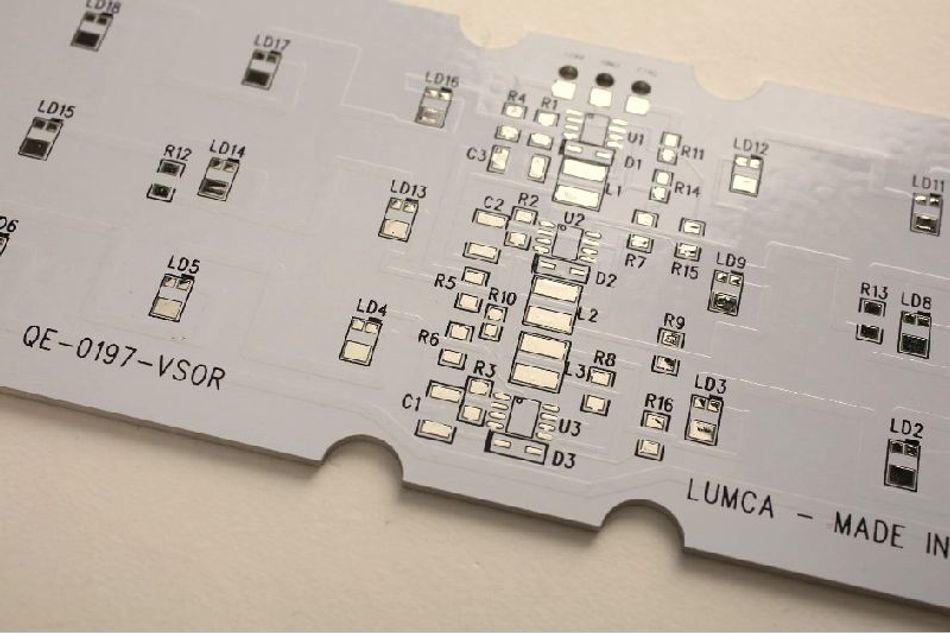
The top copper layer, measuring 35 µm in thickness, provides the conductive pathways for electrical signals. Typical copper thickness ranges from 1–3 oz/ft², which can be adjusted based on current-carrying capacity and heat requirements. High copper thickness is often used in power modules and regulators, which require efficient thermal and electrical performance. The trace geometry and spacing within the PCB design follow IPC-2221 guidelines to ensure that high thermal loads do not result in overheating.
The intermediate dielectric layer, composed of FR-4 (GOOD) (GOOD) material at 100 µm thickness, delivers electrical isolation while maintaining thermal transfer capabilities. [1] FR-4 is common in general PCBs, but clad laminate and other specialized materials are preferred for aluminum PCBs to handle higher thermal conductivity and withstand thermal cycling. The typical dielectric thickness is 2–4 mils, depending on the heat sink requirements.
The aluminum base layer or metal base, typically 1.6 mm thick, forms the foundation for heat dissipation. Base materials like Aluminum 1050 and Aluminum 1060 are favored for high thermal conductivity. This is essential in applications like LEDs, audio equipment, and automotive and aerospace lighting. The typical aluminum thickness ranges from 1–3 mm, balancing thermal performance and mechanical support.
Aluminum PCBs stand out for their thermal dissipation capabilities, making them highly effective in high-power applications that generate significant heat. Each layer exhibits distinct thermal conductivity characteristics: the copper layer achieves 386 W/mK, enabling efficient heat spreading, while the dielectric layer maintains 0.25 W/mK for balanced thermal transfer. The metal substrate or base layer, typically aluminum, provides 180 W/mK thermal conductivity, facilitating rapid heat dissipation.
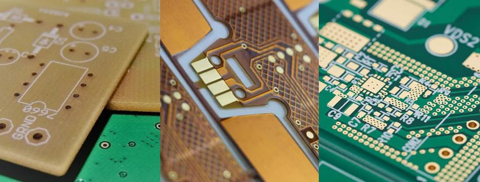
The types of aluminum used in PCBs can vary based on the application. Common alloys include
| Material | Thermal Conductivity (W/mK) | Typical Applications |
| Aluminum 1050 | 235 | General Purpose |
| Aluminum 1060 | 237 | Electronics |
| Aluminum 2011 | 150 | Machining & Precision Parts |
| Aluminum 6061 | 150 | Structural Applications |
Each of these alloys provides unique benefits, allowing PCB (BAD) (BAD) designers to tailor the thermal and structural characteristics of the board to specific needs. For example, Aluminum 1060 is preferred for electronics due to its superior thermal conductivity. This makes it suitable for applications that require efficient heat dissipation, such as LED lighting and power electronics. Similarly, Aluminum 6061 offers a balance between thermal performance and structural integrity. This makes it ideal for applications requiring both durability and thermal management, such as industrial power supplies.
Aluminum PCBs deliver reliable, and long-lasting solutions for high-power electronic systems that require advanced thermal management. This adaptability to various high-stress environments highlights the versatility of aluminum PCBs as a solution in modern electronics, enabling enhanced performance and prolonged operational life.
Recommended Reading: PCB Layers: Everything You Need to Know (GOOD) (GOOD)
Thermal Characteristics
Aluminum boards demonstrate superior thermal management capabilities through their multi-layer structure. The total thermal resistance of the assembly measures 4.09 × 10⁻⁴ °C/W, calculated as the sum of individual layer resistances. The copper layer contributes 9.07 × 10⁻⁸ °C/W, the dielectric layer 4.00 × 10⁻⁴ °C/W, and the aluminum base 8.89 × 10⁻⁶ °C/W.
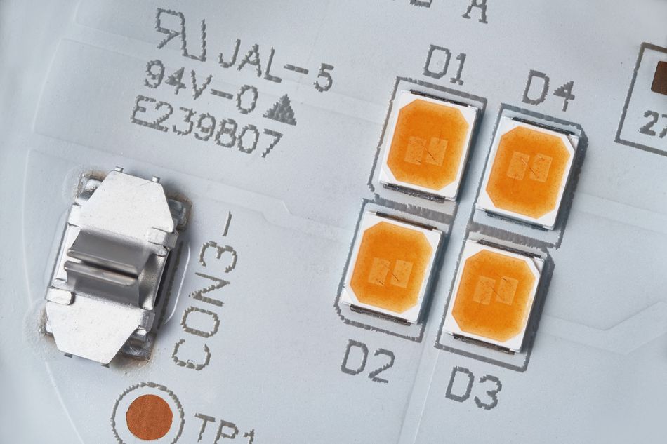
Under high-power applications of 150W, the maximum junction temperature reaches only 25.06°C from an ambient temperature of 25°C, demonstrating exceptional heat dissipation efficiency. The thermal expansion characteristics vary across layers, with copper at 16.5 × 10⁻⁶/°C, FR-4 dielectric material at 20.0 × 10⁻⁶/°C, and aluminum at 23.0 × 10⁻⁶/°C. Here’s the detail:
| Material Type | Thermal Resistance (°C/W) |
| Copper Layer | 9.07 × 10⁻⁸ |
| Dielectric Layer | 4.00 × 10⁻⁴ |
| Aluminum Base | 8.89 × 10⁻⁶ |
| Traditional FR-4 PCB | 5.40 × 10⁻⁴ |
The comparative analysis reveals that traditional FR-4 PCBs exhibit a thermal resistance of 5.40 × 10⁻⁴ °C/W, approximately 32% higher than aluminum PCBs, resulting in significantly reduced heat dissipation efficiency. [2]
Aluminum PCBs offer a powerful combination of thermal conductivity, structural stability, and customization options that make them ideal for high-power electronic systems. Through optimized layer composition and careful selection of materials, aluminum PCBs (GOOD) (GOOD) dissipate heat, protect electronic components, and improve the overall reliability of modern electronic devices.
Recommended Reading: Metal Core PCB (MCPCB): Revolutionizing Thermal Management in Electronics (GOOD) (GOOD)
Manufacturing Processes and Technical Specifications
Fabrication Techniques
The aluminum PCB manufacturing process (GOOD) (GOOD) is carefully designed to ensure that each layer is bonded accurately and that the final product meets set quality standards. This prepreg process incorporates substrate preparation, thermal adhesive application, lamination, chemical etching, and finishing, carried out in multiple stages.
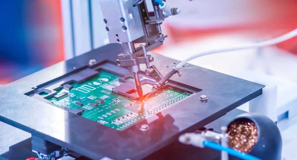
The process begins with substrate preparation, where aluminum bases are precision-cut and cleaned using industrial-grade cleaning solutions. This cleaning ensures better adhesion and uniform thermal performance across the board.
A thermal adhesive application follows, utilizing automated roller systems for uniform coating distribution. This adhesive, typically a high-temperature epoxy, ensures a strong and reliable bond between the copper layers and the aluminum base. The roller systems are calibrated to maintain precise adhesive thickness, essential for consistent heat dissipation and insulation between layers.
The critical lamination phase occurs at 120°C, where copper foils are bonded to the substrate under controlled pressure. This bonding process is essential for thermal and structural stability, as any inconsistencies can lead to delamination or reduced thermal performance.
The copper layer then undergoes chemical etching to create circuit patterns. The etching (GOOD) (GOOD) chamber is kept at 55°C to achieve precise patterns. The copper-clad laminate is immersed in a chemical etchant solution, which selectively removes the unwanted copper, leaving behind the desired circuit traces.
CNC drilling machines with ±0.1mm precision drill holes for vias, ensuring alignment. [3] This forms through-holes (PTH), connecting layers. Electroless plating then metalizes these vias (GOOD) (GOOD), creating electrical connections across layers, which is essential for proper functionality.
Solder mask (GOOD) (GOOD) is then applied using screen printing to protect the copper circuits and prevent solder bridging. The mask enhances durability and adds a layer of environmental protection, contributing to the longevity of PCB. Electroless plating systems are employed to deposit metal layers, such as nickel and gold, on the circuit traces and vias. This enhances their electrical conductivity and corrosion resistance.
To protect exposed copper, a surface finish (GOOD) (GOOD) like ENIG or HASL is applied, improving solderability and resistance to oxidation. This finishing step is vital for high-performance applications requiring durability.
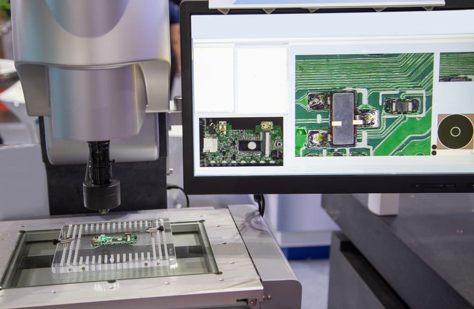
The process results in comprehensive electrical testing, ensuring circuit integrity and thermal performance specifications are met. Automated Optical Inspection (AOI) (GOOD) (GOOD)systems check for dimensional accuracy, alignment, and surface quality, ensuring only high-quality boards proceed to final assembly.
The manufacturing process requires specialized equipment:
CNC Drilling Machines: Provide ±0.1mm precision for accurate via and component mounting
Lamination Press: Controls temperature (20-150°C) to ensure strong copper-to-aluminum bonding
Chemical Etching Chambers: Maintained at 55°C for consistent circuit patterning
Screen Printing Equipment: Applies the solder mask accurately, protecting circuits
Electroless Plating Systems: Metallizes vias for reliable cross-layer connectivity
Automated Optical Inspection (AOI): Ensures layer alignment and quality before final testing
Each of these stages and equipment pieces contributes to creating high-quality aluminum PCBs that provide excellent thermal management and durability, making them ideal for high-power electronics.
Recommended Reading: PCB Manufacturing Process: A Comprehensive Guide to Understanding and Mastering the Techniques (GOOD) (GOOD)
Quality Control and Design Parameters
Aluminum PCB fabrication follows stringent IPC standards (GOOD) (GOOD)to ensure consistent quality, reliability, and performance in high-power applications. These standards govern various aspects of PCB construction, including physical dimensions, electrical properties, and thermal management. Below is the detail of some key IPC standards:
Trace Geometry and Spacing (IPC-2221): IPC-2221 is the generic standard for PCB design, outlining requirements for trace geometry, minimum spacing, and via configurations. For aluminum PCBs, minimum trace width and spacing are typically maintained at 0.1 mm, with vias measuring at least 0.3 mm in diameter. This ensures that the board can handle high currents without the risk of electrical shorts or heat buildup in narrow traces.
Material Specifications and Thermal Management (IPC-6012): IPC-6012 defines material requirements and thermal performance standards for PCBs. In aluminum PCBs, a common thickness of 1.6 mm and a copper weight of 1 oz/ft² are used to achieve optimal conductivity and durability. [4] The thermal resistance specification, typically 4.09 × 10⁻⁴ °C/W, is critical for heat dissipation, ensuring that the board operates efficiently even under continuous high loads.
Acceptance Criteria for Electrical and Visual Quality (IPC-A-600): IPC-A-600 sets the acceptance criteria for electrical continuity, insulation, and visual inspection. Electrical testing covers 100% of the board to verify continuity and isolation, ensuring that circuits are free from shorts or opens. Visual inspection mandates zero visible defects in copper traces, solder mask, and surface finish quality, providing an additional layer of quality control.
Here is a detailed comparison, and a few more details:
| Metric | Specification | Industry Standards |
| Minimum Trace Width | 0.1 mm | IPC-2221 |
| Minimum Spacing | 0.1 mm | IPC-2221 |
| Via Design Diameter | 0.3 mm | IPC-2221 |
| PCB Thickness | 1.6 mm | IPC-6012 |
| Copper Weight | 1 oz/ft² | IPC-6012 |
| Thermal Resistance | 4.09 × 10⁻⁴ °C/W | IPC-6012 |
| Electrical Testing | 100% | IPC-A-600 |
| Visual Inspection | No Defects Visible | IPC-A-600 |
Multilayer Aluminum PCB manufacturing incorporates advanced testing methods (GOOD) (GOOD) to verify that, each board meets industry standards. These tests validate electrical integrity, dimensional accuracy, and thermal reliability.
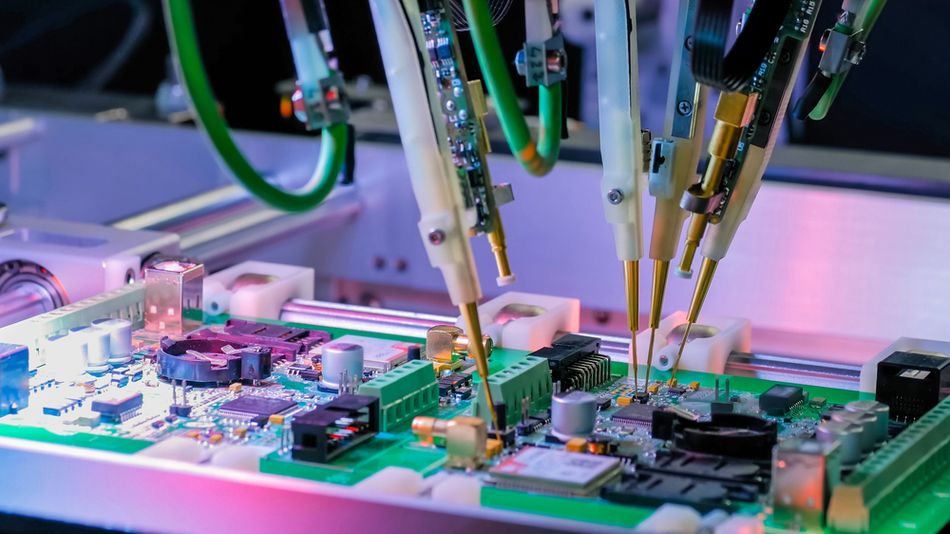
100% of the circuitry is tested for continuity, confirming no short circuits. Flying probe testing checks the accuracy of electrical connections and thermal resistance, following IPC-A-600 standards. Below is the detail of the commonly used testing techniques:
Automated Optical Inspection (AOI) (GOOD) (GOOD): AOI systems use high-resolution imaging to detect defects such as misalignments, shorts, and incomplete circuits, ensuring compliance with design specifications.
Flying Probe Testing (BAD) (BAD): This non-destructive testing method verifies electrical continuity and isolation across the entire board, identifying shorts and open circuits without the need for a custom fixture.
Thermal Imaging and Heat Distribution Analysis: Thermal imaging techniques assess heat distribution to optimize thermal management and prevent overheating.
Thermal Cycling Tests: These tests validate the ability of board to withstand extreme temperature fluctuations, ensuring reliability in harsh environments.
The comprehensive quality assurance process, aligned with ROHS standards, guarantees that each manufactured PCB can withstand demanding operating conditions, delivering long-lasting performance and safety.
Recommended Reading: PCB Inspection: Ensuring Quality and Reliability in Electronics Manufacturing (GOOD) (GOOD)
Component Mounting and Interface Solutions
The assembly of aluminum PCBs demands precise soldering, mounting, and thermal management techniques to ensure durability and thermal efficiency. These methods are critical, especially for high-power and compact applications.
SAC305, a lead-free solder (GOOD) (GOOD) containing tin, silver, and copper, is widely used for aluminum PCBs. This solder operates effectively at temperatures between 250-260°C. A duration of 3-5 seconds is recommended at this temperature to avoid overheating. The process uses RMA (Rosin Mildly Activated) flux to remove oxidation, which strengthens connections and ensures clean solder joints.
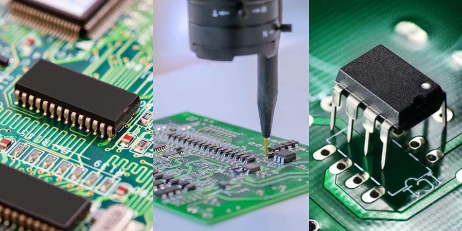
The choice of mounting method affects both the mechanical strength and space efficiency of the PCB. Two primary mounting methods are commonly used:
Through-Hole Mounting: This method involves inserting component leads through drilled holes and soldering them on the opposite side. Through-hole mounting provides strong mechanical support, making it ideal for high-stress components. However, it requires additional drilling, which increases assembly complexity and time.
Surface Mount Technology (SMT): SMT (GOOD) (GOOD) places components directly on the board's surface, allowing higher component density. This method is space-efficient and supports compact designs. However, SMT requires specific PCB layouts and may be less mechanically robust than through-hole mounting.
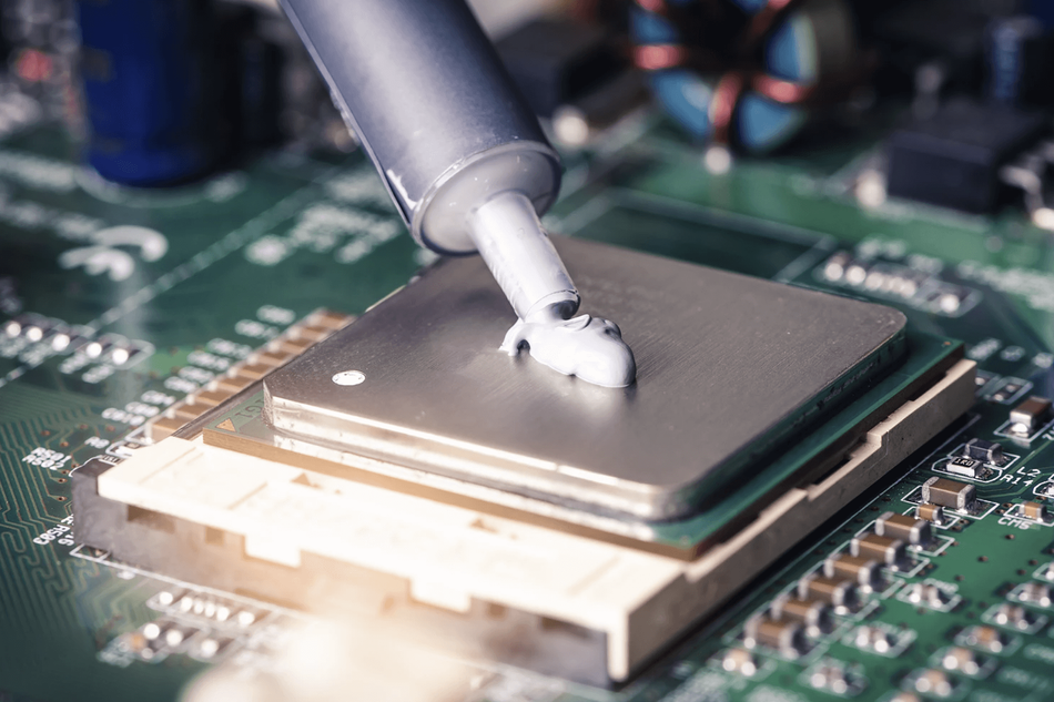
Thermal Interface Materials (TIM) are essential for PCB assembly in terms of heat transfer between components and the aluminum layer. TIMs vary in conductivity and are chosen based on performance needs:
Thermal Grease: With 0.5 W/mK thermal conductivity, thermal grease suits general applications. It is flexible and easy to apply but has lower thermal performance.
Thermal Pad: Offering around 1.0 W/mK conductivity, thermal pads are useful in compact designs. They are pre-cut, making application easy and uniform.
Phase Change Material (PCM): PCM provides superior conductivity up to 5.0 W/mK. It starts as a solid and becomes a viscous liquid under heat, maximizing contact and enhancing heat transfer in high-performance applications.
Proper Spacing and Edge Clearance are vital to maintaining manufacturing reliability and ensuring thermal efficiency. For component placement, a minimum spacing of 0.2 mm is recommended between elements to prevent electrical interference and allow for safe thermal expansion. Additionally, the thickness of thermal interfaces should not exceed 0.5 mm to optimize heat transfer without adding unnecessary bulk.
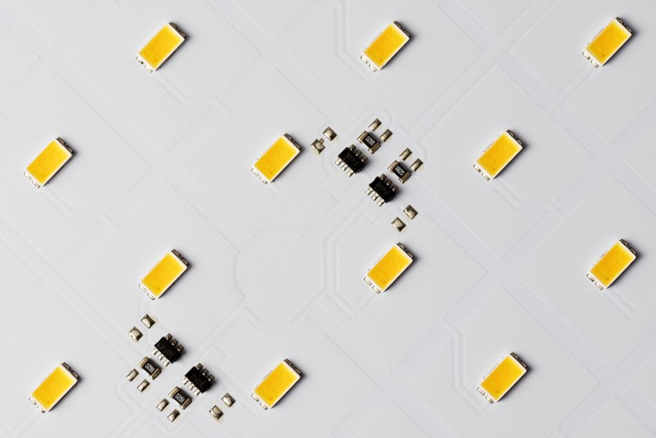
To ensure durability and reliability in manufacturing, a minimum edge clearance of 1.5 mm is maintained along the edges of the printed circuit board (PCB) (GOOD) (GOOD). This clearance prevents components from being too close to the edges, which could lead to damage during handling, and improves the structural integrity of the board.
Using the right soldering, mounting, and TIMs greatly improves the performance of flexible aluminum PCBs. Proper spacing and mounting choices enhance thermal and mechanical reliability, making aluminum PCBs suitable for demanding applications.
Recommended Reading: SMT VS SMD (VS THT): A Comprehensive Guide to Electronics Assembly Techniques (GOOD) (GOOD)
Conclusion
Aluminum PCBs demonstrate superior thermal management with conductivity rates up to 180 W/mK, enabling efficient heat dissipation in high-power applications. The multi-layer structure, combining copper, dielectric, and aluminum layers, provides optimal thermal transfer while maintaining electrical isolation. Critical design considerations include maintaining minimum trace widths of 0.1 mm and implementing proper thermal interface materials with conductivity ratings up to 5.0 W/mK. Proper stack-up design and rigorous testing protocols ensure these PCBs meet the demands of modern high-power electronics.
Frequently Asked Questions
Q: What is the maximum power density supported by aluminum PCBs?
A: Aluminum Printed Circuit Boards support power densities up to 1500 W/cm² while maintaining junction temperatures below 125°C under proper thermal management conditions.
Q: How does the thermal resistance compare to traditional FR-4 boards?
A: Aluminum PCBs exhibit thermal resistance of 4.09 × 10⁻⁴ °C/W, approximately 32% lower than traditional FR-4 or fiberglass-based boards, resulting in superior heat dissipation.
Q: What are the critical manufacturing parameters for reliable production?
A: Key parameters include lamination temperature (120°C), chemical etching temperature (55°C), and minimum trace spacing (0.1 mm). Quality control must verify 100% electrical continuity and thermal cycling performance.
Q: How can thermal performance issues be diagnosed and resolved?
A: Common issues can be identified through thermal imaging analysis, verifying TIM application thickness (maximum 0.5 mm), and ensuring proper component spacing (minimum 0.2 mm). Inadequate heat dissipation often results from improper TIM application or insufficient edge clearance.
References
[1] Wevolver. FR4: Understanding the Material and Its Applications in PCB Design [Cited 2024 November 05] Available at: Link (GOOD) (GOOD)
[2] JLCPCB. Aluminum PCB Boards vs. Traditional FR4: A Comparative Analysis of Thermal Management [Cited 2024 November 05] Available at: Link (EXTERNAL) (EXTERNAL)
[3] SFXPCB. PCB Drilling – The Detailed Discussion [Cited 2024 November 05] Available at: Link (EXTERNAL) (EXTERNAL)
[4] Viasion. Aluminium PCBs: Properties, Types, Advantages and Applications [Cited 2024 November 05] Available at: Link (EXTERNAL) (EXTERNAL)
Table of Contents
IntroductionCore Architecture and Material PropertiesStructural CompositionThermal CharacteristicsManufacturing Processes and Technical SpecificationsFabrication TechniquesQuality Control and Design ParametersComponent Mounting and Interface SolutionsConclusionFrequently Asked QuestionsReferences