Decoupling Capacitors: Mastering Power Integrity in Electronic Design
This article explores the basics, types, and key considerations surrounding decoupling capacitors in electronic systems, providing insights into mastering power integrity in modern designs.

25 Sep, 2024. 19 min read
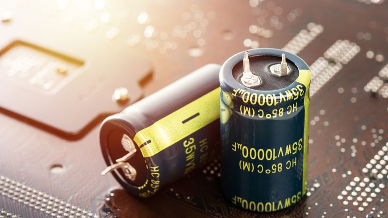
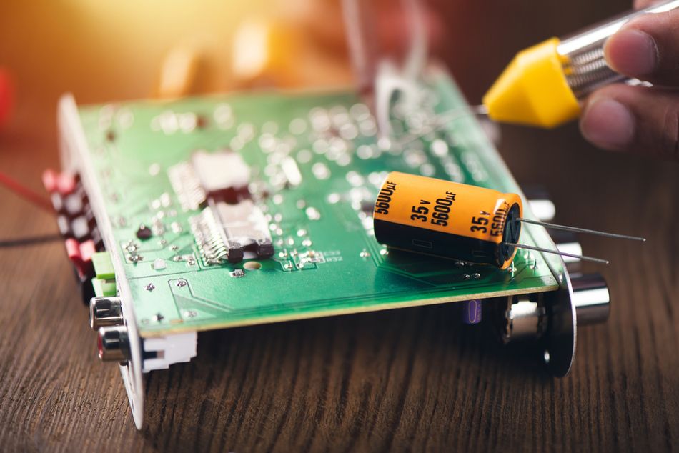
The 10,000 microfarad 35 V electrolytic capacitors, used in electronic device.
Introduction
Decoupling capacitors are fundamental components in modern electronic design, serving as the backbone of power integrity and signal quality. These small but crucial elements act as local energy reservoirs, supplying instantaneous current to integrated circuits and minimizing voltage fluctuations. Decoupling capacitors are essential for reducing electromagnetic interference (EMI), suppressing noise, and ensuring stable power distribution across printed circuit boards (PCBs).
The evolution of decoupling techniques has been driven by the relentless pursuit of faster, smaller, and more efficient electronic systems. From simple single-capacitor solutions to sophisticated multi-layer approaches, designers have continuously refined their strategies to meet the demands of cutting-edge technology. Today, effective decoupling is a critical consideration in everything from consumer electronics to automotive systems and high-performance computing. This underscores the indispensable role of decoupling capacitors in the ongoing advancement of electronic engineering.
Fundamentals of Decoupling Capacitor
What Are Decoupling Capacitors and How Do They Work?
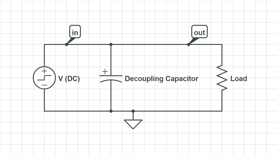
Decoupling capacitors are essential components in electronic circuits that maintain stable power supply voltages and minimize electrical noise. [1] These small but powerful devices act as local energy reservoirs, providing instantaneous current to microcontrollers or integrated circuits (ICs) when needed. By doing so, they effectively "decouple" the IC from the main power supply, hence their name.
The fundamental principle behind decoupling capacitors lies in their ability to store and release electrical charge rapidly. When an IC demands a sudden surge of current, the decoupling capacitor can supply it almost instantly, preventing voltage drops in the power supply line. Conversely, when there's excess current, the capacitor absorbs it, preventing voltage spikes.
To better understand this concept, let’s take the example of a water tank system! The main power supply is like a large water reservoir, while the decoupling capacitor is a smaller tank placed near the point of use (the IC). When there's a sudden demand for water (current), the smaller tank can provide it immediately, without waiting for water to flow from the main reservoir. This analogy illustrates how decoupling capacitors ensure a steady and responsive power supply to ICs.
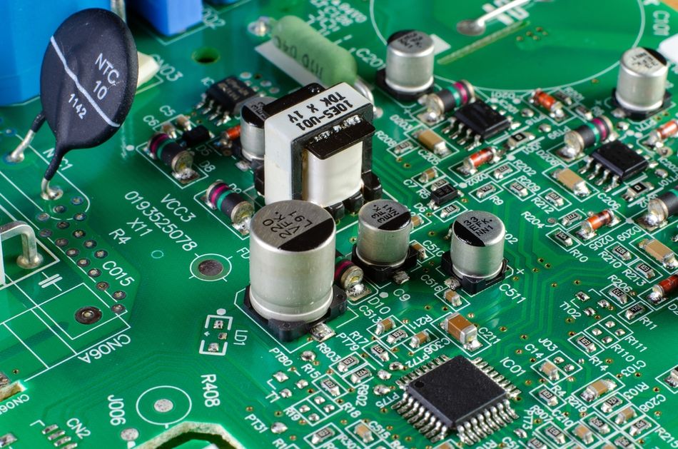
In a typical circuit, decoupling capacitors are placed as close as possible to the power pins of ICs. This proximity minimizes the inductance of the power supply traces, ensuring that the capacitor can respond quickly to the IC's current demands. The diagram above illustrates this placement, showing how the decoupling capacitor forms a local power source for the IC. This effectively filters out high-frequency noise and stabilizes the voltage supply.
By providing this local energy storage and rapid response capability, decoupling capacitors play a crucial role in maintaining signal integrity. This reduces electromagnetic interference and ensures the reliable operation of complex electronic systems. The proper selection and placement of these capacitors are critical aspects of modern electronic design, particularly as devices become faster and more sensitive to power fluctuations.
Types of Decoupling Capacitors: Choosing the Right Tool for the Job
Selecting the appropriate decoupling capacitor is crucial for optimal circuit performance. Various types of capacitors are used for decoupling, each with its own set of characteristics that make it suitable for specific applications.
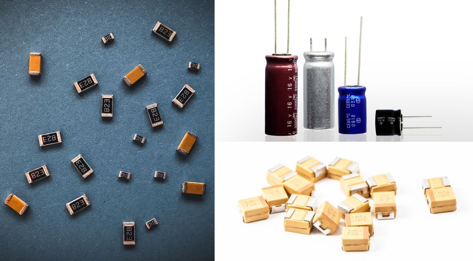
Ceramic capacitors are the most commonly used for decoupling due to their low cost, small size, and excellent high-frequency performance. They come in different dielectric types, such as X7R, X5R, and C0G (NP0), each offering different temperature stability and capacitance values.
Tantalum capacitors offer higher capacitance values in smaller packages compared to ceramics. They have low ESR (Equivalent Series Resistance) and good stability over temperature, making them suitable for applications requiring higher capacitance in a limited space. [2]
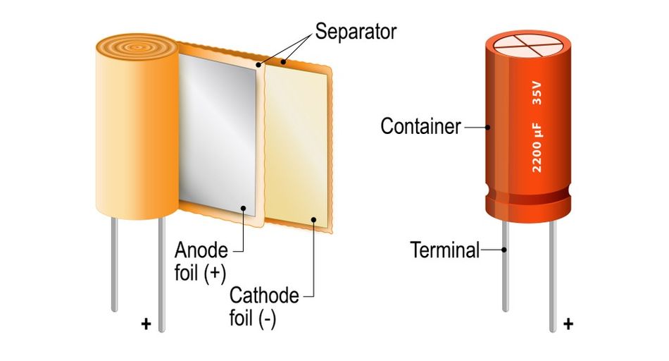
Electrolytic capacitors, both aluminium and polymer types, are used when very high capacitance values are needed. They are typically larger and have higher ESR compared to ceramic or tantalum capacitors but can provide substantial bulk decoupling.
Here’s a list of pros and cons for different types of capacitors:
| Capacitor Type | Pros | Cons |
| Ceramic | Low Cost, Small Size, Excellent High-Frequency Performance | Limited Capacitance Range, Potential for Microphonics |
| Tantalum | High Capacitance in Small Package, Low ESR, Good Temperature Stability | Higher Cost, Potential for Catastrophic Failure if Reverse-Biased |
| Aluminum Electrolytic | Very High Capacitance Values, Low Cost for Bulk Decoupling | Large Size, Higher ESR, Limited High-Frequency Performance |
| Polymer Electrolytic | High Capacitance, Lower ESR than Aluminum Electrolytic | Higher Cost, Limited Voltage Range |
When choosing a decoupling capacitor, several factors come into play:
Operating Frequency: Higher frequencies require capacitors with lower ESR and ESL (Equivalent Series Inductance).
Required Capacitance: Determined by the power requirements of the IC and the allowable voltage ripple.
Available Space: Smaller designs may necessitate the use of more compact capacitor types.
Temperature Range: Some capacitor types, like certain ceramics, can lose significant capacitance at high temperatures.
Voltage Rating: The capacitor must be rated for the circuit's operating voltage with an appropriate safety margin.
Key characteristics to consider when selecting decoupling capacitors:
Capacitance Value determines the ability of the capacitor to store and release energy.
Voltage Rating must be sufficient to handle the operating voltage of the circuit.
ESR (Equivalent Series Resistance) affects the ability of the capacitor to respond quickly to voltage transients.
ESL (Equivalent Series Inductance) can limit the effectiveness of the capacitor in decoupling high-frequency noise.
Self Resonant Frequency is the frequency at which the inductance and capacitance of a capacitor resonate.
Temperature Coefficient indicates how the capacitance changes with temperature.
Size and Form Factor are the physical dimensions and mounting style of the capacitor, compatible with the available space and the circuit layout.
Cost of the capacitor should be considered in relation to its performance and the overall system budget.
By carefully considering these factors and characteristics, engineers can select the most appropriate decoupling capacitors for their specific application. This ensures optimal circuit performance and reliability.
Recommended Reading: Capacitor Polarity: Ensuring Proper Orientation for Optimal Performance
Designing with Precision: Key Considerations for Effective Decoupling
Placement Strategies: Location, Location, Location
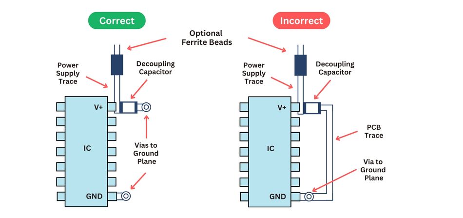
The effectiveness of decoupling capacitors is heavily dependent on their placement within a circuit. Proper positioning is crucial for minimizing parasitic inductance and ensuring that the capacitors can respond quickly to the transient current demands of integrated circuits (ICs).
The primary goal of capacitor placement is to create the shortest possible current loop between the power supply, decoupling capacitor, and IC. This minimizes the inductance of the power distribution network. This reduces voltage fluctuations and improves the overall performance of the circuit.
Several placement techniques can be employed to optimize decoupling performance:
Proximity Placement: Decoupling capacitors should be placed as close as possible to the power pins of the IC they are supporting. This reduces the length of the current path and minimizes inductance.
Symmetrical Placement: For ICs with multiple power pins, placing decoupling capacitors symmetrically around the chip can help balance the current distribution and reduce electromagnetic interference (EMI). [3]
Via-in-Pad Design: Incorporating vias directly into the pads of surface-mount capacitors can significantly reduce the inductance of the connection to power and ground planes.
Distributed Decoupling: For high-speed or complex designs, using multiple smaller capacitors distributed across the board can be more effective than a single large capacitor.
Power Plane Splitting: In multi-layer PCBs, strategically splitting power planes can help isolate noise-sensitive circuits and improve decoupling effectiveness.
Guidelines for optimal placement in different circuit designs:
For Digital Circuits: Place small (0.1μF to 0.01μF) ceramic capacitors as close as possible to each IC's power pins.
For Analog Circuits: Use larger value capacitors (1μF to 10μF) near analog ICs, and consider using separate power planes for analog and digital sections.
For High-Speed Circuits: Employ a combination of small ceramic capacitors for high-frequency decoupling and larger tantalum or electrolytic capacitors for bulk decoupling.
For Mixed Signal Designs: Isolate analog and digital grounds, using separate decoupling strategies for each section.
By carefully considering capacitor placement and employing these strategies, engineers can significantly improve the performance and reliability of their circuit designs. Proper placement ensures that decoupling capacitors can effectively suppress noise, stabilize power supply voltages, and support the fast transient currents required by modern high-speed ICs.
Sizing It Right: Calculating Capacitance Values
Determining the appropriate capacitance value for decoupling is crucial for effective power supply noise suppression and stable circuit operation.
Several factors influence the required capacitance value:
Power Supply Voltage: A higher power supply voltage generally requires a larger capacitance value to maintain adequate voltage regulation.
Maximum Allowable Voltage Ripple: The desired level of voltage ripple determines the capacitance needed to filter out unwanted fluctuations.
Load Current and Its Rate of Change: A larger load current or a rapidly changing load requires a larger capacitance to provide sufficient current to the circuit.
Operating Frequency of the Circuit: Higher operating frequencies often require smaller capacitance values to minimize the effects of parasitic inductance.
Parasitic Inductance in the Power Distribution Network: The presence of parasitic inductance can reduce the effectiveness of decoupling capacitors. A larger capacitance value may be needed to compensate for this inductance.
To calculate the appropriate capacitance value, follow these steps:
Determine the maximum current draw (ΔI) of the IC and its duration (Δt).
Specify the maximum allowable voltage ripple (ΔV).
Calculate the minimum required capacitance using the formula: C = (ΔI × Δt) / ΔV
Add a safety margin (typically 2-3 times the calculated value) to account for component tolerances and parasitic effects.
The concept of distributed capacitance plays a significant role in high-speed circuit design. Instead of using a single large capacitor, multiple smaller capacitors are distributed across the board. This approach offers several advantages:
Reduced Effective Series Inductance (ESL): Smaller capacitors generally have lower ESL, improving high-frequency performance.
Improved Response to Localized Current Demands: Distributed capacitors can respond more quickly to current needs of nearby components.
Resonance Mitigation: Multiple capacitors with different values create a more uniform impedance across a wide frequency range, reducing the risk of resonance.
Enhanced Noise Suppression: Distributed capacitance helps create a lower impedance power distribution network, effectively suppressing noise over a broader spectrum.
To implement distributed capacitance, follow these considerations:
Use a combination of capacitor values (e.g., 100nF, 10nF, 1nF) near each IC.
Place smaller value capacitors closer to the IC for high-frequency decoupling.
Use larger value capacitors for bulk decoupling, placed slightly farther from the IC.
The implications of distributed capacitance include improved power integrity, reduced EMI, and enhanced overall circuit performance, especially in high-speed and mixed-signal designs. However, it requires careful planning of PCB layout and may increase component count and assembly complexity.
Frequency Considerations: Tackling High-Speed Challenges
As electronic systems operate at increasingly higher frequencies, the behavior of decoupling capacitors becomes more complex and critical. The effectiveness of a decoupling capacitor is highly dependent on the frequency of the signals it's meant to suppress.
At low frequencies, a capacitor's impedance decreases with increasing frequency, making it an effective shunt for noise. However, as frequency increases, parasitic elements such as equivalent series inductance (ESL) and equivalent series resistance (ESR) begin to dominate the capacitor's behavior.
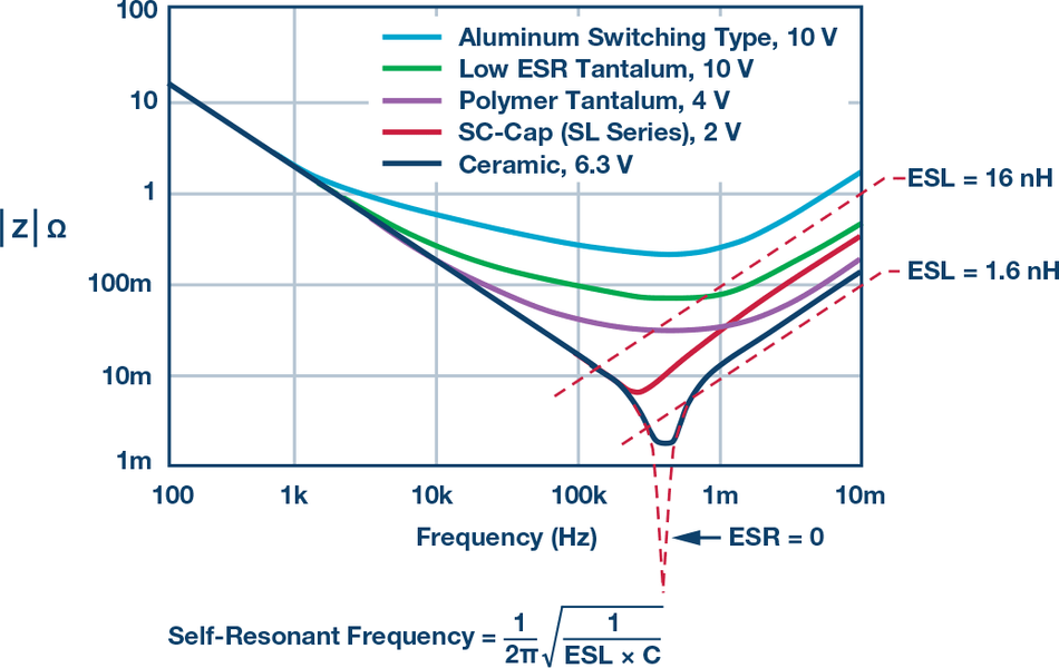
The impedance of a typical decoupling capacitor follows a U-shaped curve. At low frequencies, the impedance decreases as expected for a capacitor. However, at a certain point, the impedance reaches a minimum and then begins to increase. This minimum point is known as the self-resonant frequency (SRF).
The SRF is a crucial parameter for decoupling caps. It represents the frequency at which the capacitive reactance equals the inductive reactance of the capacitor's parasitic elements. At this point, the capacitor provides the lowest impedance and is most effective at decoupling. Above the SRF, the capacitor begins to behave more like an inductor, reducing its effectiveness for decoupling.
To tackle high-frequency decoupling challenges, several techniques can be employed:
Use Multiple Capacitors: By using capacitors of different values in parallel, a wider frequency range can be effectively decoupled. Smaller capacitors typically have higher SRFs and can handle higher frequencies.
Minimize Parasitic Inductance: Use capacitors with low ESL and place them as close as possible to the power pins of ICs. Employ via-in-pad designs and short, wide traces to reduce inductance.
Consider Specialized Capacitors: Some capacitors are designed specifically for high-frequency operation, with minimized parasitic elements.
Implement Distributed Decoupling: Place multiple smaller capacitors around the board rather than relying on a single large capacitor.
Use Ferrite Beads: In combination with capacitors, ferrite beads can provide additional high-frequency noise suppression.
Understanding these frequency-dependent characteristics is crucial for effective decoupling in high-speed circuits. By carefully selecting capacitors with appropriate SRFs and implementing proper layout techniques, engineers can ensure optimal noise suppression across a wide frequency range. This helps maintain signal integrity in even the most demanding high-speed applications.
Recommended Reading: How to Discharge a Capacitor: Comprehensive Guide
Pushing the Envelope: Advanced Decoupling Techniques
Multi-Layer Decoupling: Stacking Up Performance
Multi-layer decoupling is an advanced technique that leverages the layered structure of modern printed circuit boards (PCBs) to optimize power delivery and noise suppression. This approach involves strategically placing decoupling capacitors and power/ground planes across multiple layers of the PCB, creating a three-dimensional decoupling network.
The concept revolves around minimizing the loop inductance between power and ground connections. By utilizing multiple layers, designers can create shorter, more direct paths between decoupling capacitors and the ICs they support. This reduces the effective series inductance (ESL) of the decoupling network, enhancing its high-frequency performance.
Benefits of multi-layer decoupling include:
Improved high-frequency response due to reduced loop inductance
More efficient use of PCB real estate
Enhanced power integrity across a wider frequency range
Better isolation between different power domains
However, this approach also presents challenges:
Increased design complexity and potential for errors
Higher manufacturing costs due to additional layers and vias
Potential for increased crosstalk between layers if not properly designed
More complex impedance-matching requirements
Examples of multi-layer decoupling implementations include:
Buried capacitor technology, where thin dielectric layers are embedded within the PCB
Interstitial via arrangements that connect capacitors to power/ground planes on inner layers
Distributed capacitance using closely spaced power and ground planes
A cross-sectional diagram of a multi-layer PCB with decoupling capacitors would typically show:
Multiple copper layers alternating between signal, power, and ground planes
Surface-mounted decoupling capacitors on the top and bottom layers
Vias connecting the capacitors to internal power and ground planes
Buried vias connecting internal capacitors or planes
Thin dielectric layers between closely spaced power and ground planes for distributed capacitance
Interstitial vias providing short connections between layers
This layered approach creates a low-impedance power distribution network that effectively suppresses noise across a wide frequency spectrum. This pushes the boundaries of what's possible in high-speed and high-density electronic designs.
Active Decoupling: The Next Frontier
Active decoupling represents an advanced approach to power supply noise reduction in electronic systems. Unlike traditional passive decoupling techniques, active decoupling employs active electronic components to dynamically counteract power supply fluctuations.
At its core, active decoupling uses a feedback mechanism to sense voltage variations on the power rail and generate an opposing signal to cancel out these fluctuations. [4] This is typically achieved through a combination of high-speed operational amplifiers, transistors, and control circuits. The active nature of this approach allows for more precise and responsive noise suppression compared to passive methods.
The key differences between active and passive decoupling include:
Bandwidth: Active decoupling can operate effectively over a wider frequency range, potentially extending into the GHz domain.
Adaptability: Active systems can adjust their response based on real-time power supply conditions.
Impedance: Active decoupling can achieve lower effective impedance across a broader frequency spectrum.
Advantages of active decoupling include:
Enhanced noise suppression performance, especially at high frequencies
Reduced dependence on board layout and parasitic elements
Potential for smaller form factors by reducing the number of decoupling capacitors required
Ability to address specific noise profiles through customized circuit designs
However, active decoupling also comes with limitations:
Increased complexity and cost compared to passive solutions
Additional power consumption by the active components
Potential for instability if not properly designed
Reliability concerns due to the increased component count
Examples of active decoupling implementations include:
Low-Dropout (LDO) Regulators with integrated active noise cancellation
Feedforward error correction amplifiers in power distribution networks
Switched-capacitor circuits that dynamically adjust decoupling capacitance
Active electromagnetic interference (EMI) cancellation systems
The ongoing development of high-speed, low-power active components is expected to further enhance the viability and adoption of active decoupling solutions in future designs.
Recommended Reading: Types of SMD Components: A Comprehensive Guide
Real-World Impact: Practical Applications of Decoupling Capacitors
Taming EMI in Consumer Electronics
Decoupling capacitors play a crucial role in reducing electromagnetic interference (EMI) in consumer electronics. These devices are essential for maintaining signal integrity and ensuring compliance with electromagnetic compatibility (EMC) standards.
In smartphones, decoupling capacitors are strategically placed near critical components such as the processor, RF modules, and display drivers. For example, in a typical smartphone design, multiple small ceramic capacitors (0.1μF to 1μF) are placed close to the application processor's power pins. This arrangement significantly reduces the EMI generated by the high-speed switching of the processor, which can interfere with sensitive RF circuits used for cellular communication.
Laptops benefit from the extensive use of decoupling capacitors to manage EMI across various subsystems. The power delivery network for the CPU and GPU often employs a combination of bulk electrolytic capacitors and smaller ceramic capacitors for effective decoupling across a wide frequency range. This approach helps minimize EMI that could otherwise affect Wi-Fi and Bluetooth performance or cause display artefacts.
To illustrate the effectiveness of proper decoupling, consider the following hypothetical before-and-after EMI measurements for a consumer tablet device:
Before decoupling optimization:
Radiated emissions at 1 GHz: -35 dBm
Conducted emissions on power lines at 150 kHz: -70 dBμV
After implementing optimized decoupling:
Radiated emissions at 1 GHz: -55 dBm (20 dB reduction)
Conducted emissions on power lines at 150 kHz: -85 dBμV (15 dB reduction)
Effective decoupling significantly reduces EMI, ensuring regulatory compliance and improving device performance. This reduces radiated emissions and prevents interference with other devices, while also decreasing conducted emissions to minimize noise in the power grid.
In smart home devices, such as voice-controlled speakers, decoupling capacitors are critical for isolating sensitive audio circuits from digital noise. By implementing a combination of bulk decoupling (10μF to 100μF) near the power input and distributed smaller capacitors (0.01μF to 0.1μF) across the board, designers can achieve a cleaner audio output and improved voice recognition performance.
The effective use of decoupling capacitors in consumer electronics not only ensures regulatory compliance but also enhances product reliability. This improves battery life by reducing power waste, and contributes to the overall user experience by minimizing interference-related issues.
Ensuring Reliability in Automotive Electronics
Decoupling capacitors play a crucial role in maintaining the reliability and performance of automotive electronic systems. In modern vehicles, where the number of electronic control units (ECUs) and sensors continues to grow, effective decoupling is essential for ensuring electromagnetic compatibility (EMC), signal integrity, and overall system stability.
The automotive environment presents unique challenges for electronic components:
Temperature Variations: Automotive electronics must function reliably in extreme temperatures, from -40°C to 125°C or higher. Decoupling caps need to maintain their characteristics across this wide range.
Vibration and Mechanical Stress: Constant vibration from the engine and road conditions can affect component connections and PCB integrity. Decoupling capacitors must remain securely connected and functional under these conditions.
Electromagnetic Interference (EMI): The dense packaging of electronic systems in vehicles, combined with high-power components like electric motors, creates a challenging EMI environment.
Voltage Transients: Automotive power systems can experience high voltage spikes and drops, requiring robust decoupling to protect sensitive components.
To address these challenges, automotive engineers employ specialized decoupling solutions:
High-Temperature Ceramic Capacitors: X7R or X8R dielectric capacitors are often used for their stability across wide temperature ranges. [5]
Redundant Decoupling: Critical systems may use multiple decoupling capacitors in parallel to ensure continued operation even if one fails.
Low-ESR Capacitors: These are crucial for maintaining effective decoupling at high frequencies, common in automotive communication buses.
Distributed Decoupling: Placing smaller capacitors close to ICs, combined with larger bulk capacitors near power entry points, helps manage both local and system-wide noise.
Examples of decoupling applications in critical automotive systems include:
Engine Control Units (ECUs): Precise decoupling is essential for maintaining accurate sensor readings and control signals.
Advanced Driver Assistance Systems (ADAS): Camera and radar modules require clean power supplies for accurate object detection and tracking.
Infotainment Systems: Effective decoupling helps prevent noise from digital circuits from interfering with audio quality or touchscreen responsiveness.
Case Study: Improving EMC in Electric Vehicle Inverters
A major electric vehicle manufacturer faced challenges with electromagnetic emissions from their high-power inverters interfering with other vehicle systems. By implementing a multi-layer decoupling strategy, they achieved significant improvements:
Used a combination of high-capacity film capacitors for bulk decoupling and smaller ceramic capacitors for high-frequency noise suppression.
Implemented embedded capacitance in the PCB design, creating a low-impedance power distribution network.
Utilized specialized automotive-grade capacitors with high ripple current ratings and temperature stability.
The results showed a 15 dB reduction in conducted emissions across the 150 kHz to 30 MHz frequency range, bringing the inverter into compliance with fixed automotive EMC standards. This improvement eliminated interference issues with the vehicle's radio and navigation systems, enhancing overall reliability and customer satisfaction.
This case demonstrates how advanced decoupling techniques can solve complex EMC challenges in automotive applications, contributing to the development of efficient electric vehicles.
Optimizing Performance in High-Speed Digital Systems
In high-speed digital systems, decoupling capacitors play a critical role in maintaining signal integrity by providing localized charge storage and minimizing power supply noise. As clock speeds and data rates continue to increase, effective decoupling becomes increasingly challenging and crucial for system performance.
Decoupling in high-speed circuits serves several key functions:
Reducing power supply noise and voltage fluctuations
Minimizing electromagnetic interference (EMI)
Supporting fast transient currents required by digital ICs
Maintaining stable reference voltages for high-speed signaling
For multi-gigahertz designs, advanced decoupling techniques are essential:
Distributed Decoupling: Multiple smaller capacitors are placed strategically across the PCB, closer to the ICs they support. This reduces the effective inductance and provides better high-frequency performance.
Multilayer Capacitors: Low-inductance multilayer ceramic capacitors (MLCCs) are preferred for their excellent high-frequency characteristics.
Power Plane Segmentation: Separating power planes for different voltage domains helps isolate noise and improve decoupling effectiveness.
Embedded Capacitance: Using thin dielectric materials between power and ground planes creates distributed capacitance throughout the PCB.
Active Decoupling: For extremely high-frequency applications, active circuits can be employed to dynamically compensate for voltage fluctuations.
Examples of decoupling strategies in high-speed systems include:
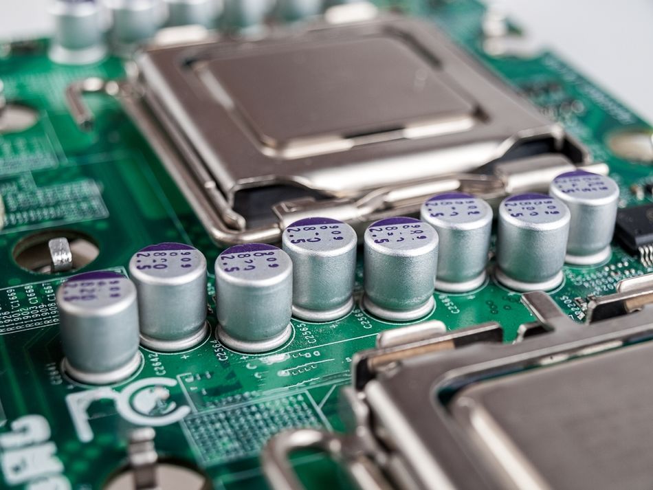
Processors: Modern CPUs often employ a hierarchical decoupling network. This involves large bulk capacitors near the voltage regulators, medium-sized capacitors distributed around the processor package, and small, high-frequency capacitors directly under the die.
FPGAs: High-performance FPGAs require careful decoupling of multiple power domains. Designers often use a combination of 0.1μF and 0.01μF capacitors placed as close as possible to each power pin, with larger bulk capacitors (10μF to 100μF) near power entry points.
High-Speed Memory Systems: DDR4 and DDR5 memory interfaces require precise decoupling to maintain signal integrity at data rates exceeding 3200 MT/s. This often involves placing small (0.1μF to 1μF) capacitors near each memory chip and termination network.
Before-and-After Comparison of Signal Quality:
Before proper decoupling:
Signal rise time: 150 ps
Jitter (peak-to-peak): 40 ps
Power supply noise: 150 mVpp
After implementing optimized decoupling:
Signal rise time: 120 ps (20% improvement)
Jitter (peak-to-peak): 25 ps (37.5% reduction)
Power supply noise: 50 mVpp (66.7% reduction)
These improvements in signal quality directly translate to better system performance, increased timing margins, and improved reliability in high-speed digital systems. The reduced jitter and power supply noise allows for higher data rates and more robust communication. The faster rise times enable shorter bit periods and higher overall throughput.
Recommended Reading: Supercapacitor FAQ
Troubleshooting Decoupling Dilemmas: Common Issues and Solutions
Identifying Decoupling-Related Problems
Inadequate decoupling in electronic circuits can lead to a variety of issues that affect system performance and reliability. Recognizing the symptoms of decoupling problems is crucial for effective troubleshooting and optimization.
The common symptoms include:
Excessive noise on power rails
Intermittent system instability or crashes
Unexplained EMI emissions
Signal integrity issues (e.g., jitter, ringing, or distortion)
Voltage drops during high-current transients
Crosstalk between adjacent signal lines
Failure to meet EMC compliance standards
Measurement techniques for assessing decoupling effectiveness include:
Time-Domain Oscilloscope Measurements: Observe voltage ripple on power rails during circuit operation. Look for excessive noise or voltage drops during load transients.
Spectrum Analysis: Use a spectrum analyzer to identify noise components and resonances in the power distribution network. Pay attention to the harmonics of clock frequencies and switching regulators.
Network Analysis: Employ a vector network analyzer to measure the impedance of the power distribution network across a wide frequency range. Compare results to target impedance profiles.
Near-Field EMI Scanning: Use near-field probes to locate sources of electromagnetic emissions, which can indicate areas of inadequate decoupling.
Examples of waveforms or spectra indicating decoupling problems:
Time-Domain Voltage Ripple:
Adequate Decoupling: < 50mV peak-to-peak ripple
Inadequate Decoupling: > 200mV peak-to-peak ripple with sharp transients
Frequency-Domain Power Spectrum:
Adequate Decoupling: Smooth noise floor with minimal spikes
Inadequate Decoupling: Prominent spikes at clock frequencies and their harmonics, possible resonance peaks
Impedance Profile:
Adequate Decoupling: Smooth curve below target impedance across frequency range
Inadequate Decoupling: Impedance peaks exceeding the target, especially at high frequencies
EMI Scan Result:
Adequate Decoupling: Low, uniform emissions across the board
Inadequate Decoupling: Hot spots of high emissions near ICs or power traces
To effectively implement decoupling, refer to the datasheet or tutorials of your microcontroller for specific recommendations. The schematic will guide you on the placement of decoupling capacitors near the Vcc and GND pins.
Typically, a combination of larger decoupling capacitors (10µF to 100µF) near the power supply and smaller bypass capacitors (0.01µF to 0.1µF) directly at the power pins of the microcontroller is used. The package size of the capacitors should be chosen based on the available board space and routing constraints. By following these guidelines, you can ensure optimal power integrity and reliable performance in your electronic designs.
Recommended Reading: How Do Circuit Boards Work: A Comprehensive Guide to the Heart of Electronics
Conclusion
Decoupling capacitors are fundamental components in modern electronic design, playing a crucial role in maintaining power integrity and signal quality. From consumer electronics to automotive systems and high-speed digital circuits, proper decoupling is essential for optimal performance, reliability, and electromagnetic compatibility. The evolution of decoupling techniques, including multi-layer approaches and active decoupling, has kept pace with the increasing demands of advanced electronic systems.
As technology continues to push the boundaries of speed and integration, the importance of effective decoupling strategies cannot be overstated. By understanding the principles and techniques associated with decoupling, engineers can create more robust, efficient, and reliable electronic designs that meet the ever-increasing demands of the digital age.
Frequently Asked Questions
Q: What is the primary purpose of a decoupling capacitor?
A: The primary purpose of a decoupling capacitor, or bypass cap is to provide a local source of charge for integrated circuits. This reduces power supply noise and maintains stable voltage levels during rapid current demand changes.
Q: How do I choose the right value for a decoupling capacitor?
A: The value of a decoupling capacitor depends on factors such as the operating frequency, current requirements, and allowable voltage ripple. Generally, a combination of larger bulk capacitors (1-100μF) and smaller high-frequency capacitors (0.01-0.1μF) is used. Specific calculations based on the circuit's needs are often necessary for optimal selection.
Q: How does temperature affect decoupling capacitor performance?
A: Temperature can significantly impact capacitor performance, especially for ceramic capacitors. Some dielectric types, like X7R, can lose up to 80% of their capacitance at high temperatures. It's crucial to consider the operating temperature range and choose capacitors with appropriate temperature coefficients for the application.
Q: What is the difference between decoupling and bypass capacitors?
A: The terms are often used interchangeably, but there's a subtle difference. Decoupling capacitors typically refer to larger capacitors that provide bulk charge storage and low-frequency noise suppression. Bypass capacitors usually refer to smaller, high-frequency capacitors placed very close to IC power pins for local, high-speed transient suppression.
Q: Is it always necessary to use multiple decoupling capacitors for each IC?
A: While it's common practice to use multiple capacitors, it's not always necessary for every IC. Low-power or low-speed devices may function adequately with a single well-chosen capacitor. However, for high-speed or noise-sensitive applications, using multiple capacitors of different values helps cover a wider frequency range and improves overall decoupling effectiveness.
References
[1] IC Components. Comprehensive Guide to Decoupling and Bypass Capacitors: Mechanisms, Applications, and Differences [Cited 2024 September 20] Available at: Link
[2] Wevolver. Capacitor Polarity: Ensuring Proper Orientation for Optimal Performance [Cited 2024 September 20] Available at: Link
[3] E+I Elektrotechnik. Influence of the IC Power Supply and Decoupling Capacitor Arrangement on Electromagnetic Emission [Cited 2024 September 20] Available at: Link
[4] ResearchGate. Active Power Decoupling Control for Single-Phase Current Source Rectifier Based on Emulating LC Resonator [Cited 2024 September 20] Available at: Link
[5] ResearchGate. Achieving Ultrabroad Temperature Stability Range with High Dielectric Constant and Superior Energy Storage Density in KNN–based Ceramic Capacitors [Cited 2024 September 20] Available at: Link
Table of Contents
IntroductionFundamentals of Decoupling CapacitorWhat Are Decoupling Capacitors and How Do They Work?Types of Decoupling Capacitors: Choosing the Right Tool for the Job Designing with Precision: Key Considerations for Effective DecouplingPlacement Strategies: Location, Location, LocationSizing It Right: Calculating Capacitance ValuesFrequency Considerations: Tackling High-Speed ChallengesPushing the Envelope: Advanced Decoupling TechniquesMulti-Layer Decoupling: Stacking Up PerformanceActive Decoupling: The Next FrontierReal-World Impact: Practical Applications of Decoupling CapacitorsTaming EMI in Consumer ElectronicsEnsuring Reliability in Automotive ElectronicsOptimizing Performance in High-Speed Digital SystemsTroubleshooting Decoupling Dilemmas: Common Issues and SolutionsIdentifying Decoupling-Related ProblemsConclusionFrequently Asked QuestionsReferences