Flex PCB Design Guidelines for a Tougher Flex
Due to the properties of flexible PCBs and their unique applications, a whole different set of design rules apply to flex boards. In this article, we highlight some basic design guidelines, tips and tricks that every flex PCB designer should know.
06 Jun, 2024. 4 minutes read

The freedom to bend and twist in all directions while being relatively frail calls for greater emphasis towards the mechanical properties of flex PCB design. Every element that goes into the design could impact the flexibility, durability, assembly and cost of flex PCBs which can have a major influence on the choice of materials, layout and placement of parts.
Why choose flex printed circuit boards?
There are typically two reasons for choosing a flex substrate over a rigid one. Number one is of course their flexible nature, allowing them to fit into non-planar spaces and facilitate motion. The second is to take advantage of the paper-like thinness that has enabled a generation of thin handheld devices - the most obvious example being to replace bulky cables. As with all designs, the application's specific requirements dictate which design measures should be enforced.
Challenges of designing flex PCBs
The advantages of flex PCBs do not come without their (big) fair share of challenges. Since the layers of flex PCBs are typically held together with adhesives, holding all the pieces together as the board is bent and tugged in various directions is a major challenge of FPC design. Pads are more likely to lift or tear in response to mechanical stresses and layers of a flex PCB can peel and detach at high bend frequencies and angles. This is further exacerbated by poor temperature-resistant adhesives and flex materials which demand extra care during assembly.
For high flex requirements, designers must take into account the design of every layer and strike a compromise between flexibility and durability. As the number and thickness of copper layers increase, this undoubtedly impacts the flexibility of the board. Various measures can be taken to reduce thickness and increase flexibility in high bend areas such as by removing excess coverlay and copper.
Excess flexibility can be an issue too. Bending in areas populated with components can cause additional stress on solder joints. Thus, it makes sense to adopt a rigid-flex board style design whereby bending is restricted to certain areas. For simple designs, by strategically placing stiffeners in high-density areas, designers can reduce stress on solder joints without the extra expense of rigid-flex boards.
Flex PCB Design Guidelines
Coverlay Design
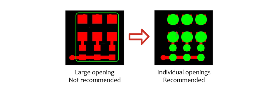
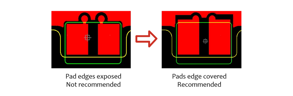
Pad encapsulation can be utilized for the pads of chip resistors, capacitors and LEDs etc. by rounding the coverlay opening. This creates anchor points that hold the pad to the substrate. Do not allow openings to expand too far out in high density areas to maintain solder mask dams between pads and prevent solder bridges from forming.

Manually soldered parts
For manually soldered parts such as microphones and speakers, elongate the pad under the coverlay to help hold the pad to the substrate and prevent the pad from lifting.
Onboard Connectors
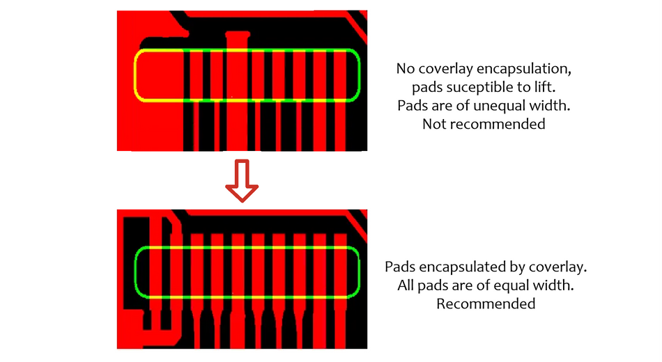
Extra anchoring is important for onboard connectors since they could be subjected to strong pulling forces. Strengthen them by elongating the pads under the coverlay and utilizing teardrops to prevent pads from tearing. This encapsulates the pads and helps prevent the pads from lifting. Ensure the ground pad is the same size as the other pads to promote even heat distribution during soldering and reduce solder defects.
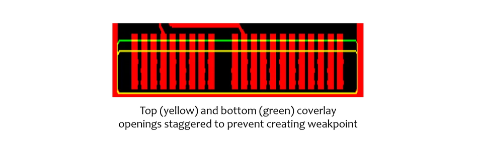
For double-sided edge connectors with gold fingers on both sides, the coverlay openings should be staggered to avoid creating a weak point. Stagger top and bottom coverlay openings by 0.5mm, with the opening facing the mainboard shorter than the opening facing outwards. Coverlay should cover the base of the gold fingers for added protection and plated holes and half holes can be added to fingers to improve solder joint strength.
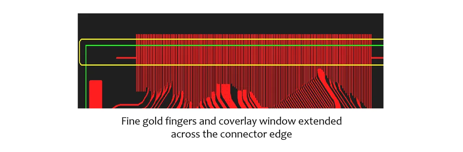
For thin gold fingers, extend the pads and the coverlay window across the board edge by 0.5mm to help hold them in place during punch pressing.
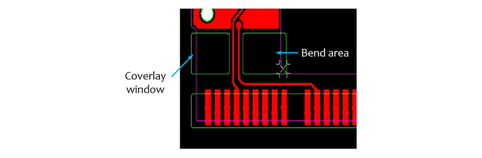
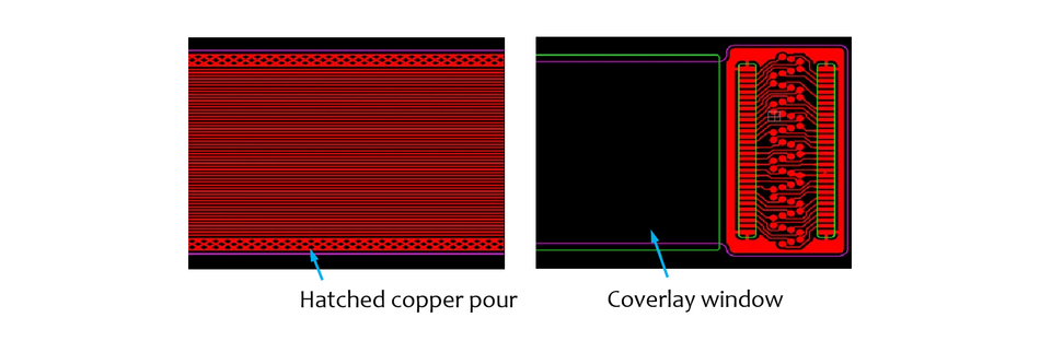
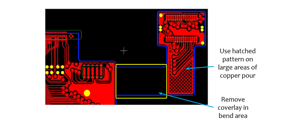
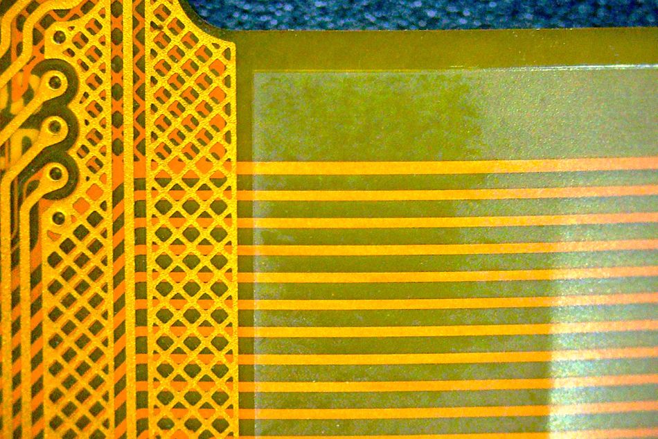
To help increase flexibility in the bend area, coverlay and copper pour can be removed from the bend area where no copper is present and solid copper pour can be substituted for a hatched (mesh) pattern.

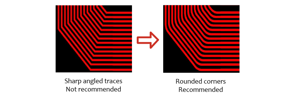
Use Curved Traces
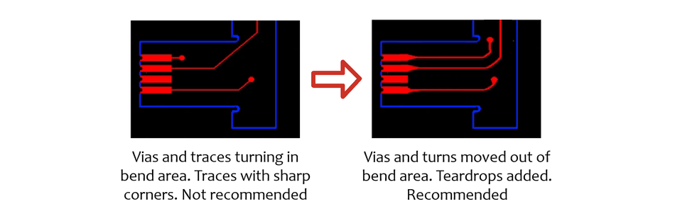
Do not place vias in the bend area and keep traces in the bend area wide and as straight as possible, perpendicular to the intended fold. Use curved traces to reduce areas of weakness.
Dome Switch Design
Add teardrops where the traces connect to the pad and use thick traces when possible. As a rule of thumb, traces should not be less than 0.2mm in width.

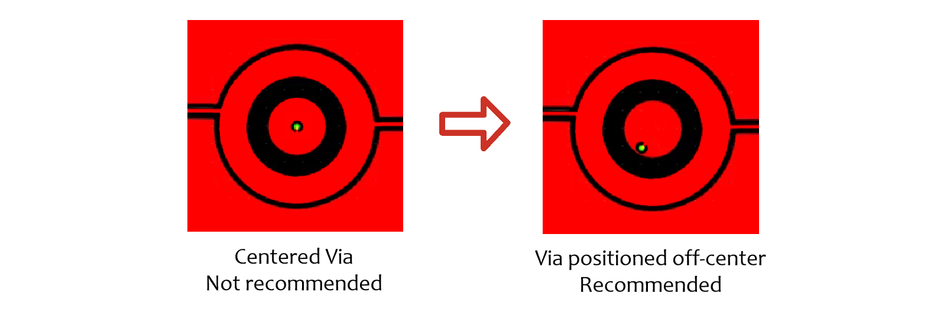
Do not position vias in the center of dome switch contacts as the via may interfere with the electrical connection when pressed.
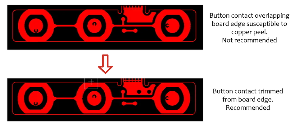
Button traces that overlap over the board edge should be trimmed 0.15mm from the board edge to protect the copper and stop peeling.
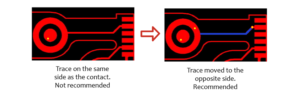
For side buttons, place traces on the opposite side of the button if possible.
Flex PCB Outline Design
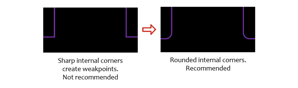
Round internal corners near bend areas to protect against tear and preserve longevity.
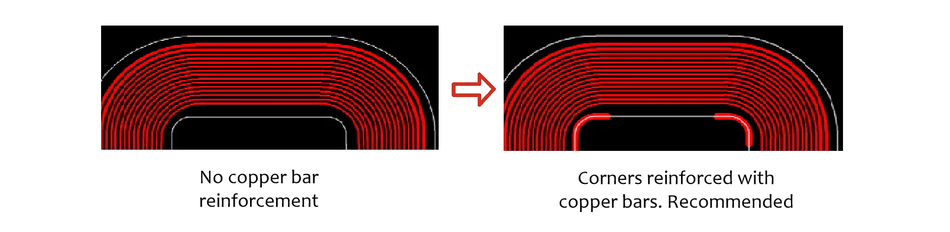
For added strength on inner corners, consider adding reinforcement in the form of copper rails.
The list above contains just some of the design considerations PCB designers should take into account when designing flexible printed circuit boards. As we have seen, much care goes into maintaining flexibility and strength at the same time, which at times can appear to be pulling at the two ends of the same piece of string. A compromise has to be struck and designers prioritize properties most important to the flex board's application and environment in the field.
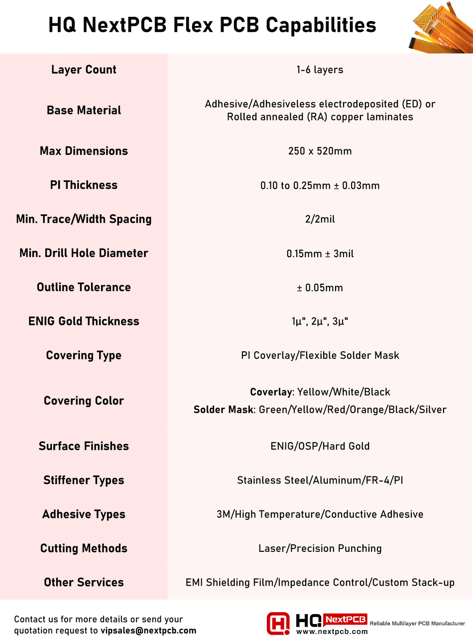
Tougher applications call for tougher electronics. HQ NextPCB is a reliable multi-layer PCB manufacturer and assembly house based in China whose capabilities include rigid, flex and rigid-flex printed circuit boards. Their flex circuit board capabilities go up to 6 layers with a wide selection of stiffeners, adhesives, EMI shielding and cutting methods available. Get in touch for a quotation.