How Advanced Circuit Boards Enhance Device Functionality
Advanced PCBs use features like microvias and fine-line traces to achieve ultra-high wiring density that leads to miniaturization and improved device performance

13 Mar, 2025. 4 minutes read
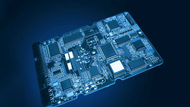
Printed Circuit Boards (PCBs) have come a long way since their inception in the early 20th century, culminating in advanced or High-Density Interconnect (HDI) PCBs, which offer superior performance—in very small packages—for modern electronics.
Early circuit boards were rudimentary and consisted of point-to-point wiring. The 1940s saw the introduction of single-sided PCBs, where conductive traces were etched onto insulating substrates. By the 1950s, plated-through holes became common, improving circuit density and paving the way for PCBs to become widespread in consumer goods. The 1980s brought multilayer PCBs, allowing for even greater complexity and miniaturization.
Advanced PCBs emerged as a response to the demand for higher performance in smaller packages. These boards utilize microvias, blind and buried vias, and fine-line traces to achieve higher wiring densities than other types of PCBs. Unlike previous board types, advanced circuits use sequential lamination, allowing for multiple layers of interconnects.[1]
The Challenge of Making Advanced Circuit Boards
The advantages of advanced printed circuit technology include better signal integrity, reduced electromagnetic interference (EMI), and improved thermal performance, as well as reduced size and weight. Because of these benefits, they can be used in high-value applications like smartphones, medical devices, and aerospace electronics. Their compact design also enables lower power consumption and faster signal transmission.
However, just as the development of the first PCBs in the 1940s presented a huge challenge for electrical and electronics engineers, today the efficient production of advanced PCBs is a major test, with only a small number of companies capable of building advanced printed circuit technology. One major difficulty in advanced circuit PCB production is the likelihood of conductive path defects. These defects are difficult to repair, resulting in a high scrap rate, making the production process less economically feasible.
Advanced printed circuit technology must therefore:
Offer a very high level of precision
Be capable of printing very fine conductive line widths
Offer a means of repairing broken conductive lines
A technology like Ultra-Precise Dispensing (UPD) from XTPL can be used directly for the miniaturization of conductive circuits, creating submicron conductive paths and circuits with the highest levels of path density. Most importantly, UPD excels at open defect repair, as it can print on any type of conductive or non-conductive substrate, including glass, flexible foil (e.g. Kapton, PET, PEN, PDMS), and silicon wafers, in addition to 2.5D substrates.
Technological Innovations with Advanced Circuit Boards
Advanced printed circuit boards improve the functionality of modern technological devices by enabling miniaturized, high-performance designs with a high level of electrical performance. Their fine line traces, microvias, and multiple layers allow for increased component density, reducing size while boosting signal integrity and reliability.
Possible applications include:
IoT Devices: Advanced PCBs enable miniaturized, power-efficient IoT sensors and communication modules, ensuring seamless data transmission in smart homes and industrial automation.
Advanced Sensors: High-precision sensors in medical devices, autonomous vehicles, and environmental monitoring benefit from the high-speed signal transmission and low interference of advanced circuit PCBs.
Smartphones and Wearable Electronics: Advanced circuit boards allow for thinner, lighter smartphones and wearables with high processing power, better battery efficiency, and superior wireless connectivity.
Automotive Electronics: Modern vehicles rely on HDI PCBs for ADAS (Advanced Driver Assistance Systems), infotainment, and electric vehicle battery management.
Medical Devices: Pacemakers, hearing aids, and imaging equipment use advanced circuit boards for compact, high-performance electronics, improving patient outcomes.[2] These PCBs must be able to withstand sterilization and emit minimal heat.
By reducing weight, enhancing electrical performance, and enabling miniaturization, advanced or HDI PCBs are key to many important technological advancements. In the near future, they may be essential for quantum computing hardware, which could exploit advanced printed circuit technology to enhance connectivity and reduce interference in superconducting circuits. Additionally, space and defense technologies could use these PCBs for radiation-resistant, high-performance electronics in next-generation satellites and aerospace systems.
New Possibilities for PCBs
Advanced circuit boards are at the core of modern electronics, enabling miniaturization, enhanced electrical performance, and higher reliability. Their fine-line traces, microvias, and multilayer structures allow for compact yet high-functioning designs in industries like healthcare, automotive, and telecommunications.
However, manufacturing challenges such as line defects demand innovative solutions. Technologies like XTPL’s Ultra-Precise Dispensing (UPD) can overcome these challenges by enabling high-precision printing of submicron conductive paths and defect repair on a variety of substrates. The technology has already demonstrated its viability in areas like autonomous driving interconnect packaging and flexible hybrid electronics.[3][4]
As electronic devices continue to shrink and demand greater performance, advanced PCBs will become even more important. From IoT and medical devices to future quantum computing and aerospace applications, these cutting-edge circuit boards will drive the next generation of technological breakthroughs. Finding better ways to print them is therefore a matter of the highest priority for engineers.
Resources
[1] Jha P, Patel M, Kumar R, Hegde RK, Pandya S. Quality Compliance of HDI PCBs for Space Use. In2024 IEEE Space, Aerospace and Defence Conference (SPACE) 2024 Jul 22 (pp. 1019-1022). IEEE.
[2] Stampanoni M. Sophisticated HDI flexible substrates for advanced applications. Circuit World. 2003 Sep 1;29(3):14-7.
[3] Wang T, Lu CW, Feng E, Yang YJ, Chang CY, Cheng PP, Lie F, Cheng A, Huang HY, Koh M, Wiatrowska A. A Novel FOPLP Structure with Chip First & RDL First Process for Automotive chip application. In2024 IEEE 74th Electronic Components and Technology Conference (ECTC) 2024 May 28 (pp. 1868-1871). IEEE.
[4] Ma S, Dahiya AS, Christou A, Zumeit A, Dahiya R. High‐Resolution Printing‐Based Vertical Interconnects for Flexible Hybrid Electronics. Advanced Materials Technologies. 2024:2400130.