OSAT Semiconductor Services: The Backbone of Outsourced Chip Assembly & Testing
OSAT (Outsourced Semiconductor Assembly and Test) firms package, assemble, and test chips for fabless companies and foundries. As chip complexity rises, they boost efficiency, lower costs, and speed market entry for AI, IoT, and HPC. This article reviews OSAT fundamentals, players, and trends.

17 Mar, 2025. 33 minutes read

No time now? Save for later.
We only use your email to send this link. Privacy Policy.
Introduction
Every microchip’s journey from a silicon wafer to a fully functional electronic component relies on a crucial stage: assembly and testing. This is where Outsourced Semiconductor Assembly and Test (OSAT) companies come in. They specialize in cutting fabricated semiconductor wafers into individual chips, packaging them, and rigorously testing them to ensure quality and reliability. By handling these critical post-fabrication processes, OSAT providers enable semiconductor companies to streamline production and focus on chip design and innovation.
In today’s fabless semiconductor landscape, OSAT providers are indispensable. Even tech giants like Apple rely on OSAT partners, such as ASE in Taiwan, to package their processors. By outsourcing these back-end processes, chip designers and wafer fabs can optimize efficiency, creating a highly specialized global supply chain—where chips are designed in one country, fabricated in another, and assembled elsewhere. As semiconductor technology advances, the demand for smaller, more powerful, and energy-efficient chips has skyrocketed, making OSAT firms more crucial.
One of the most significant innovations in this space is advanced packaging, where OSAT firms stack multiple chips together to enhance performance. Technologies like fan-out wafer-level packaging (FOWLP), chiplets, and system-in-package (SiP) are driving breakthroughs in AI, IoT, and high-performance computing (HPC). However, OSAT companies face growing challenges, including supply chain disruptions, rising material costs, and the need for constant technological upgrades. As global semiconductor demand increases, the role of OSAT in ensuring reliable, high-performance chips will only grow, shaping the future of the electronics industry.
The Critical Role of OSAT Companies in the Semiconductor Ecosystem
OSAT (Outsourced Semiconductor Assembly and Test) companies hold a crucial position in the semiconductor value chain, serving as the back-end manufacturing partners for chip producers. Their primary role is to provide third-party IC packaging and testing services, ensuring that silicon dies—after fabrication—are transformed into fully functional semiconductor components ready for integration into electronic devices.
OSAT providers function as specialized partners that enable the mass production of reliable semiconductor products. Without them, many chip design firms—especially fabless startups—would struggle to bring innovations to market at scale. By bridging the gap between wafer fabrication and final product integration, OSATs enhance efficiency, drive innovation, and ensure the seamless operation of the global semiconductor supply chain.
The Evolution of OSATs: From IDM to Specialization
In the early days, most semiconductor companies operated as Integrated Device Manufacturers (IDMs), managing everything from chip design and wafer fabrication to assembly and testing under one roof. However, as the industry evolved, it became highly disaggregated:
Fabless companies focus on chip design.
Foundries specialize in wafer fabrication.
OSAT providers handle assembly and testing.
This shift allowed companies to reduce costs, improve efficiency, and focus on core competencies. OSAT firms emerged to support fabless companies lacking in-house packaging capabilities and IDMs looking to outsource overflow production or cut operational expenses.
Recommended reading: Chips and Wafers: What's the Difference?
Why OSATs Are Essential
Cost Efficiency & Flexibility
OSATs eliminate the need for semiconductor firms to invest heavily in their own assembly and testing facilities. Instead, they can scale production up or down based on market demand while benefiting from OSATs' economies of scale.Maximizing Front-End Fab Output
Wafer fabrication is extremely expensive, and fabs operate most efficiently when focused solely on producing wafers. OSATs take over the time-consuming packaging and testing process, ensuring that front-end fabs maintain high utilization rates and increase overall chip supply.Innovation & Expertise
OSAT companies are not just service providers—they are technology pioneers. They continuously develop advanced packaging techniques (e.g., 3D chip stacking, fan-out wafer-level packaging) and cutting-edge testing methodologies that benefit the entire industry. Fabless companies, in particular, gain access to these innovations without having to invest in R&D themselves.
Theoretical Concepts and Working Principles of OSAT
It’s important to recognize the intricate balance OSAT providers strike between innovation and efficiency. OSAT providers must navigate a range of complex processes, from advanced packaging technologies to cutting-edge testing methods, ensuring that semiconductor components meet the highest standards of performance. What sets these companies apart is their ability to adapt to ever-evolving industry demands, integrating new methodologies and staying ahead of the curve. Here are core principles that empower OSAT providers to support the semiconductor industry’s rapid advancements and ensure that each chip is ready for the real world.
Semiconductor Packaging
Packaging is the process of placing a bare silicon die into a protective housing and providing it with electrical connections to the outside world. The package (which can be made of plastic molding compound, ceramic, or other materials) shields the delicate chip from physical damage, corrosion, and contamination, while the package’s pins, pads, or balls serve as the interface that allows the chip to be soldered onto a circuit board and communicate with other components. In essence, packaging connects the chip to its environment and ensures it can be handled and used in devices.
IC Assembly Steps
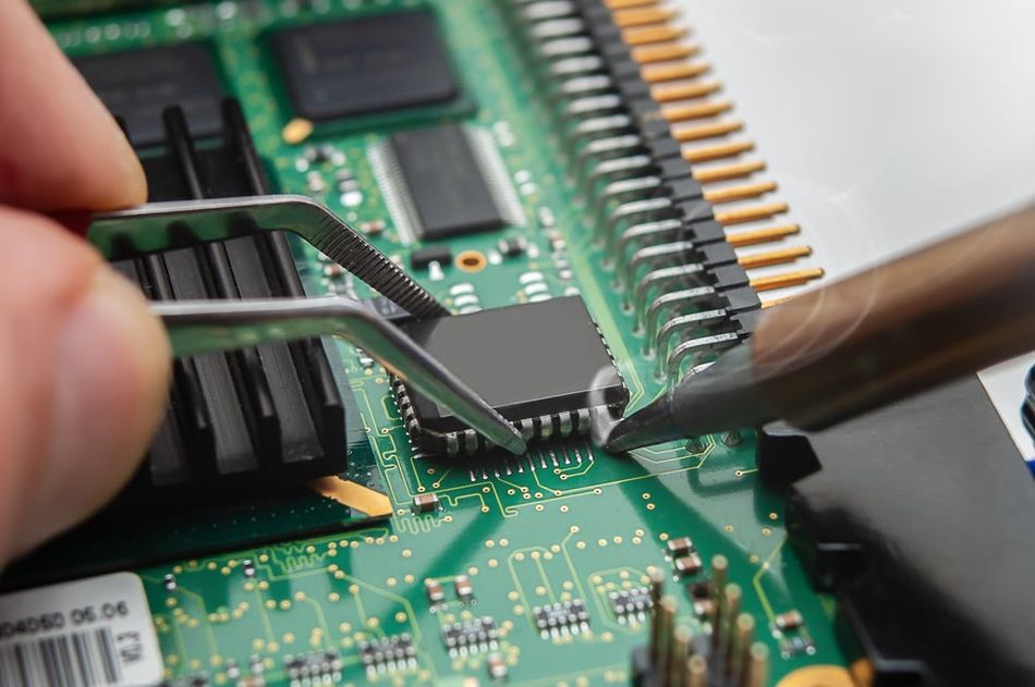
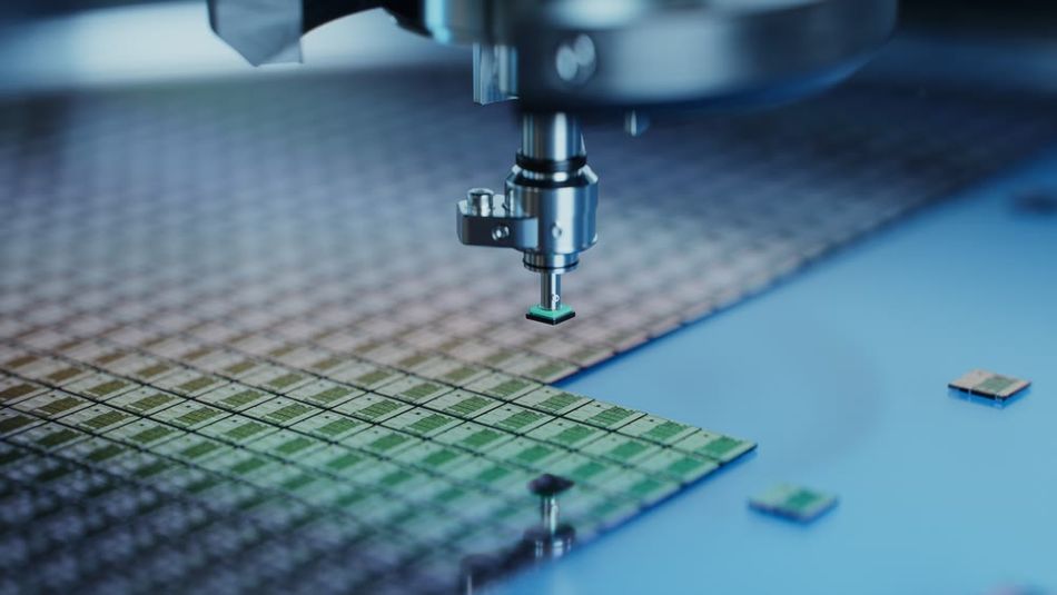
In OSAT factories, the assembly process typically includes multiple steps. First, wafer dicing is performed – the completed wafer is cut into individual dies (chips). Each die is then attached to a substrate or lead frame (for example, using epoxy or solder). Next comes interconnection: either wire bonding or flip-chip bonding is used to connect the circuitry on the die to the package leads. Wire bonding uses fine metal wires (often gold or copper) to stitch between the chip and lead frame pads, one bond at a time, whereas flip-chip (controlled collapse chip connection) attaches the die face-down using solder bumps, enabling many connections in parallel.
After interconnection, the assembly is encapsulated – for most consumer chips, this means encasing it in a hard epoxy molding that forms the final chip package outline. Some packages also involve attaching a metal lid or heat spreader (common in high-performance processors). Finally, the packaged units are singulated (separated if they were molded in groups), and any external features like solder balls (for BGA – Ball Grid Array packages) are added. The outcome of assembly is a finished semiconductor component, e.g., a CPU in a BGA package or a power IC in a plastic SOIC (Small Outline IC) package.
Semiconductor Testing
Following assembly, extensive testing is conducted in two main phases: wafer probe (or wafer sort) and final test. Wafer probing, typically performed either at the fab or by OSAT before packaging, involves using needle-like probes to touch the pads of each die on the wafer to conduct basic electrical tests. Once packaged, the final test phase takes place, utilizing automated test equipment (ATE) to ensure the chips meet their specifications.
OSAT companies are equipped with large test floors housing sophisticated ATE machines from suppliers like Advantest and Teradyne. These machines quickly run functional tests, speed binning, and other performance checks to verify that the chip meets design requirements. For highly integrated chips, such as system-on-chip (SoC) or system-in-package (SiP) devices, system-level tests may also be performed, simulating real-world conditions by running actual software loads to assess their performance in a real environment. Chips that fail any test are either marked for rejection or recycled, while functional chips are forwarded for delivery.
Recommended reading: Semiconductor Resilience with Innovations in Testing Techniques and Packaging
Reliability Screening
In addition to basic functional testing, OSATs also conduct reliability and burn-in tests to ensure the long-term durability and performance of the chips. Burn-in testing subjects the chips to elevated temperatures and voltages for extended periods, encouraging early failures and identifying "infant mortality" defects. This process eliminates weak units that would otherwise fail prematurely in the field. OSATs also perform various environmental stress tests, such as temperature cycling (alternating between hot and cold temperatures to simulate thermal expansion), humidity exposure, and drop tests, tailored to meet customer-specific requirements. Many OSAT providers have dedicated reliability labs to carry out these critical assessments, ensuring that packaged devices can withstand the demanding conditions of their intended applications. For example, automotive chips must meet rigorous quality and reliability standards before they can be used in vehicles.
Quality Control and Yield Management
During both assembly and testing, OSAT companies implement stringent quality control measures at every stage. This includes optical inspections, where automated vision systems verify wire bond placement and other critical details, as well as electrical parametric tests to ensure proper function. Statistical process control is also used to monitor yields. Given that OSATs handle high volumes—testing billions of units annually for major customers—a small improvement in yield can lead to significant cost and time savings. OSATs collaborate closely with their customers, providing detailed yield data and failure analysis. If issues arise upstream, such as with chip design or wafer fabrication, this feedback loop ensures that corrective actions are taken, driving continuous improvement across the entire supply chain.
The core working principle of OSAT services is to take the outputs of semiconductor fabrication and transform them into finished, reliable products. Through meticulous packaging processes and exhaustive testing, OSATs add value by making chips usable and dependable. The technologies used range from relatively simple (e.g., classic wire-bond plastic packages) to highly advanced (e.g., multi-die stacked packages with thousands of connections). A strong theoretical foundation in materials science, electrical testing, and thermal/mechanical engineering underpins these operations – and OSAT companies have developed deep know-how in all these areas to meet the evolving needs of the semiconductor industry.
Recommended reading: How are Semiconductors Made? A Comprehensive Guide to Semiconductor Manufacturing
OSAT vs. IDM: Business Models and Supply Chain Strategies
The semiconductor industry today primarily operates under two paradigms for assembling and testing chips: the IDM model and the OSAT model. Understanding their differences is key to appreciating why OSATs have become so prevalent.
Integrated Device Manufacturer (IDM) Model
IDMs are vertically integrated semiconductor companies that handle all production steps in-house, from wafer fabrication to packaging and testing. Examples of IDM's include Intel, Samsung, and Texas Instruments. These companies invest in their own assembly and test facilities and typically develop internal expertise for those processes. The IDM approach offers tight control over the manufacturing flow and can be beneficial for proprietary or highly sensitive technologies. For instance, if an IDM is packaging a cutting-edge processor using unique techniques, they may prefer to keep that knowledge internally. However, maintaining in-house packaging/testing also means bearing all the associated costs (equipment, facilities, manpower) and ensuring high utilization of those resources to be cost-effective.
Outsourced Semiconductor Assembly and Test (OSAT) Model
In this model, a chip company, often fabless (meaning it designs chips but doesn’t own its own semiconductor fabrication plant), outsources the assembly and testing of its chips to specialized external providers. OSAT companies, acting as merchant vendors, aggregate demand from multiple clients, enabling them to achieve economies of scale in packaging and testing services. They cater to any customer in need of back-end services, whether that customer is fabless or an Integrated Device Manufacturer (IDM) looking to outsource part of its operations. The typical business arrangement involves the chip company sending its completed wafers (or individual dies) to the OSAT, which then returns the packaged, tested chips ready for distribution. This approach allows chip companies to avoid the heavy capital expenditures associated with maintaining assembly and testing facilities while providing them with the flexibility to scale up or down quickly based on demand or technological changes in packaging. Essentially, it allows companies to "buy" packaging and testing services as needed, optimizing both cost-efficiency and agility.
The decision between the IDM (Integrated Device Manufacturer) and OSAT (Outsourced Semiconductor Assembly and Test) models is largely driven by economics, scale, and business focus. Building an advanced packaging facility is a capital-intensive endeavor that is only practical for companies with either high-volume production or specialized requirements. Fabless companies, which focus primarily on chip design, outsource both wafer fabrication to foundries and assembly/test to OSATs. Even many IDMs rely on OSATs for specific product lines, overflow capacity, or when their internal facilities are at full capacity or lack specialized packaging capabilities.
One notable trend is the global dominance of the OSAT model in terms of volume. Studies indicate that more than 81% of the world’s semiconductor assembly, testing, and packaging are handled in Asia, predominantly by OSAT companies. This concentration in Asia, particularly in Taiwan, China, Malaysia, Singapore, and South Korea, is driven by the labor-intensive nature of packaging and the need to reduce costs. For example, even major IDMs like Texas Instruments and Intel have moved the bulk of their assembly and test operations overseas, despite being U.S.-based companies. This reflects the fact that, even for companies that could adopt the IDM model, the advantages of using OSATs for cost efficiency and scale often outweigh keeping assembly in-house.
The OSAT model provides semiconductor companies with significant flexibility. Companies can choose OSATs that specialize in particular packaging techniques, such as ultra-thin packaging for mobile chips, and can switch providers based on the specific needs of each project. If there’s an unexpected spike in demand, leveraging multiple OSATs helps alleviate production bottlenecks. Furthermore, by serving a broad customer base, OSAT companies can spread the cost of expensive equipment, such as advanced lithography tools or high-end testers, across multiple jobs, reducing the cost per chip for everyone. This collaborative approach has been mutually beneficial, allowing chip companies to focus on design and innovation while OSATs concentrate on perfecting back-end manufacturing.
However, relying on OSATs also brings certain risks and dependencies. Geopolitical tensions, supply chain disruptions, or logistical challenges in Asia can impact the operations of OSAT facilities and, consequently, disrupt the product shipments of fabless companies. This concentration of OSAT capacity in East Asia has raised concerns in other regions, prompting government initiatives like the U.S. CHIPS and Science Act of 2022. These initiatives aim to strengthen domestic advanced packaging capabilities and reduce reliance on overseas OSAT providers. Some IDMs are reassessing their approach, weighing the cost savings of outsourcing to OSATs against the control and security that comes with keeping packaging in-house.
The decision to choose between an IDM or OSAT model is a strategic one for semiconductor firms, and the trend in recent decades has heavily favored outsourcing. The merchant OSAT model currently handles the majority of global chip assembly and testing, playing a crucial role in the growth of the semiconductor industry and enabling the fabless semiconductor revolution. While the IDM model still holds importance for high-end processors or mission-critical chips, and as a safeguard against over-reliance on external partners, many companies adopt a hybrid approach. Both models continue to coexist, serving different needs and contributing to the resilience and efficiency of the semiconductor supply chain.
Key OSAT Service Providers and Their Impact on the Supply Chain
The OSAT (Outsourced Semiconductor Assembly and Test) industry, though home to numerous companies globally, is predominantly shaped by a few dominant players who command a significant portion of the market. These major OSAT providers hold considerable influence over the semiconductor ecosystem, particularly in how and where chips are packaged and tested. Leading companies such as ASE, Amkor, and JCET not only play a central role in maintaining the efficiency and resilience of the semiconductor supply chain but also drive innovation and expansion within the industry. For example, when ASE introduces a new advanced packaging line, it offers a substantial advantage to numerous fabless companies that can now leverage this new capability for their own chip designs. Similarly, Amkor or JCET’s global expansion—such as establishing new plants in emerging semiconductor hubs—enables local companies to access top-tier assembly and testing services without needing to rely on overseas facilities.
Equally important is the mutual interdependence that exists between OSATs and chip companies. OSATs rely on a steady flow of chips to package, while chip companies depend on OSATs to handle the packaging and testing processes. This symbiotic relationship has been successful, but it requires ongoing coordination between the two parties—such as sharing roadmaps and keeping each other informed of production needs. To ensure a seamless back-end process, many OSATs work closely with their customers during the chip design phase, advising on critical Design for Packaging and Test (DFX) considerations. This collaboration is becoming even more crucial as packaging technology grows more intricate and demanding. In the following sections, we’ll dive deeper into the complex nature of modern semiconductor packaging and highlight real-world examples of how OSAT services are utilized in action.
Practical Implementations: Packaging, Testing, and Reliability in Action
In a real-world scenario, the role of OSAT services is critical in bringing a semiconductor product to market. Here’s a breakdown of how OSATs would typically handle a chip, like a Wi-Fi/Bluetooth combo chip for smartphones, from assembly to delivery:
1. Package Selection and Co-Design
The collaboration between the fabless semiconductor company and the OSAT begins early in the chip’s development. Together, they select the best packaging solution for the chip. For a wireless connectivity chip like this, a compact package is necessary to fit into the limited space of smartphones. The OSAT might recommend a QFN (Quad Flat No-leads) package or a wafer-level chip scale package (WLCSP) if size is a priority. OSAT engineers help define the best design for the substrate, which ensures proper signal integrity, particularly important for high-frequency chips like Wi-Fi/Bluetooth combos.
2. Wafer Back-End Preparation
After the chip is fabricated at the foundry, it undergoes back-end preparation. This may involve wafer thinning to make the die thin enough for packaging or adding solder bumps for flip-chip configurations. Once the wafer is ready, the foundry will dice the wafer into individual dies, which are sent to the OSAT for packaging.
3. Assembly Process
The assembly process is where the die is mounted onto the package. If the package is a QFN, the die is glued onto a pad, and fine gold wires are bonded from the die pads to the leadframe leads. In more advanced scenarios, such as a flip-chip BGA (Ball Grid Array), the die is flipped face-down onto the substrate with micro solder balls connecting the die to the circuit. OSATs typically employ automated systems to speed up processes like wire bonding, with advanced bonding machines capable of placing dozens of wires per second. Molding machines encapsulate the chips, ensuring the protective casing is securely formed around each package. Depending on the method, the OSAT may process many chips at once in an array format, which is more efficient than handling each chip individually.
4. Testing and Bin Sorting
Once assembled, the chips are tested. OSATs use automated test handlers that insert chips into test sockets connected to automated test equipment (ATE) for various tests, such as RF performance (e.g., transmit power, receiver sensitivity) and digital functionality. If the chips pass the tests, they may be sorted into different bins based on performance criteria (e.g., power consumption, signal strength). Chips that do not meet the required standards are rejected. The OSAT might also mark each chip with an identifier or laser engrave it to indicate its quality.
5. Reliability Testing
For new chips, especially those used in critical applications (like automotive-grade chips), the OSAT will perform additional reliability testing. These tests ensure that the chips can withstand real-world conditions over their lifespan. Reliability tests could include burn-in tests, where chips are subjected to high temperatures for an extended period, or accelerated humidity exposure (pressure cooker tests). Automotive-grade chips often undergo 100% burn-in to meet stringent reliability standards. These tests are essential to ensure that the packaged chip will function reliably under demanding conditions.
6. Final Logistics
Once the chips pass all testing and reliability checks, the OSAT will handle the logistics for distribution. The chips are typically packaged in tape-and-reel or trays, depending on the customer’s needs, and shipped to the customer’s distribution center or directly to the original equipment manufacturer (OEM). Some OSATs offer complete turnkey solutions, managing not only the assembly and testing but also the logistics and inventory management, ensuring the chips reach the OEMs efficiently.
This end-to-end process ensures that semiconductor companies can focus on their core strengths (such as chip design) while relying on OSATs to handle the complex, labor-intensive tasks of packaging, testing, and logistics. Through collaboration and specialized services, OSATs contribute significantly to reducing time-to-market, improving product reliability, and optimizing supply chain efficiency for chip companies.
Real-World Example: Advanced Packaging in Action
A prime example of OSAT (Outsourced Semiconductor Assembly and Test) expertise in action is in high-performance computing chips. Take a GPU (graphics processing unit) utilizing 2.5D packaging with High-Bandwidth Memory (HBM). In this setup, the GPU die and multiple HBM memory dies are mounted on a silicon interposer—an intermediary layer that enables high-speed interconnects. This entire assembly is then packaged in a single BGA (Ball Grid Array).
While a foundry like TSMC may fabricate the GPU and interposer, an OSAT provider such as ASE or Amkor takes on the critical task of integrating the GPU and HBM onto the interposer and packaging the final module. This process demands exceptional precision, involving advanced techniques like flip-chip bonding and thermocompression bonding. Beyond assembly, the OSAT conducts rigorous testing—not just on the GPU itself but on the entire multi-die module—to ensure seamless operation. By successfully executing these intricate packaging solutions, OSATs enable the next generation of chiplet and multi-die architectures, turning cutting-edge semiconductor designs into scalable, manufacturable products.
Ensuring Reliability: OSAT's Role in Automotive Chips
Now, consider an automotive sensor chip assembled by an OSAT. Given the stringent reliability demands of the automotive industry, these chips must endure extreme stress tests—such as 1,000 hours of high-temperature operating life testing and thermal cycling from -40°C to 125°C, repeated hundreds of times. OSATs set up specialized test chambers and custom boards to perform these stress evaluations, collecting real-time data on parameter shifts, potential failures, and package degradation. This data is invaluable for chip manufacturers, allowing them to refine designs and processes, ensuring the final product meets the industry’s 10-15 year lifespan requirements. In this role, OSATs are not just manufacturers—they serve as quality gatekeepers and key data providers in the semiconductor supply chain.
Bridging Innovation and Manufacturing
From standard microcontrollers to the most advanced processor modules, OSATs handle a diverse range of packaging and testing needs. Their expertise transforms theoretical semiconductor designs into tangible, reliable products. Whether assembling a miniature chip for a wearable device or integrating a multi-chip module for data centers, OSATs continuously balance performance, cost, size, and reliability. Their ability to adapt to evolving technologies ensures that semiconductor innovations become real-world solutions, ready for mass deployment.
Supply Chain Considerations and the Global Impact of OSAT
The rise of OSAT providers has significantly shaped the global semiconductor supply chain. Several key considerations emerge when looking at how OSAT services impact the broader industry and world:
1. Geographic Concentration: Efficiency vs. Risk
The semiconductor assembly and test industry is heavily concentrated in Asia, with Taiwan, China, South Korea, Malaysia, and Singapore hosting the majority of OSAT facilities. This clustering offers cost advantages, proximity to leading foundries like TSMC, and seamless integration with electronics manufacturing hubs. Taiwan’s OSAT giants—ASE, SPIL, and others—along with facilities in Southeast Asia, dominate the global chip packaging market.
However, this concentration presents a significant risk. Natural disasters (earthquakes, typhoons), geopolitical tensions, or pandemics could severely disrupt operations, causing widespread delays. The COVID-19 pandemic exposed these vulnerabilities, as packaging and testing became a bottleneck in the semiconductor supply chain, contributing to the 2020-2021 global chip shortage. As a result, chipmakers and governments are prioritizing supply chain diversification, with efforts to establish packaging and test facilities in regions like the U.S. and Europe to mitigate risks.
2. OSAT’s Role in the Fabless-Foundry Model
OSAT services are a critical link in the fabless semiconductor business model, where companies like Qualcomm and NVIDIA design chips but outsource manufacturing. The typical process flows as follows:
Chip design → Wafer fabrication (foundry) → Assembly & test (OSAT) → Final product delivery.
Any disruption at the OSAT stage can ripple across the supply chain, affecting product launch timelines. Fabless companies work closely with OSAT providers, often stationing engineers on-site, sharing forecasts, and coordinating quality control. The just-in-time nature of electronics manufacturing means that OSAT facilities must deliver on schedule—delays could mean missing critical production windows for products like smartphones set to launch for the holiday season.
Additionally, OSATs must stay aligned with foundry innovations. When foundries introduce new wafer processes, such as advanced chiplet architectures, OSATs must be prepared with compatible packaging solutions. This interdependence ensures that semiconductor advancements translate into market-ready products.
3. Industry Influence: Multi-Billion Dollar Contracts
Top OSAT providers secure long-term contracts with major chipmakers, embedding themselves into critical supply chains. For instance, Apple’s $44.95 billion deal with ASE highlights the scale of OSAT’s involvement in high-volume consumer electronics. Such agreements influence OSAT investment decisions, encouraging facilities to expand advanced packaging capabilities.
The surge in demand for automotive semiconductors further illustrates OSAT’s influence. As electric vehicles and autonomous driving systems require more reliable, high-performance chips, OSATs like Amkor and ASE have invested in specialized facilities and testing capabilities to meet stringent automotive standards. These investments shape industry trends, determining which packaging technologies gain widespread adoption.
4. OSAT’s Role in Emerging Markets
The rise of OSAT providers has driven economic growth in regions like Taiwan, Malaysia, and China’s Jiangsu and Guangdong provinces. These facilities create thousands of skilled jobs and foster local expertise in microelectronics, helping to position these countries as key players in the global semiconductor ecosystem. Governments actively compete to attract OSAT investment, recognizing that assembly and test facilities serve as a gateway into high-tech manufacturing.
In contrast, the U.S. has a relatively limited OSAT infrastructure—just ~46 OSAT facilities compared to hundreds in Asia. This gap has prompted strategic initiatives, such as the CHIPS Act, to bolster domestic semiconductor manufacturing and packaging capabilities. Increasing onshore OSAT capacity is seen as a way to enhance supply chain resilience and national security.
5. Logistics and Lead Time Challenges
The OSAT process introduces additional logistical complexity. A typical semiconductor might follow this journey:
Designed in California
Fabricated in Taiwan
Packaged and tested in Malaysia
Assembled onto a PCB in China
Integrated into a final product and shipped worldwide
Each step involves shipping costs, border crossings, and potential delays. Export controls, such as restrictions on certain semiconductor technologies, further complicate logistics. To streamline operations, some foundries and OSATs have formed close partnerships. For example, TSMC has integrated packaging solutions like InFO and CoWoS, allowing wafers to transition directly into advanced packaging processes, reducing delays and improving time-to-market.
6. Quality Assurance and Supply Chain Traceability
OSAT providers serve as the final checkpoint before semiconductor devices enter mass production. A single defect in chip packaging—such as a weak internal connection—could lead to product failures, costly recalls, and reputational damage. To mitigate this risk, OSATs enforce strict traceability systems, tracking every chip through its processing history, from the machines used to the operator handling the lot.
This data is critical for identifying and isolating defective batches before they reach the market. In high-reliability sectors like automotive and aerospace, OSATs perform rigorous stress testing to ensure chips can endure extreme conditions—such as thermal cycling from -40°C to 125°C for thousands of hours. Their role in maintaining chip reliability directly impacts industries ranging from consumer electronics to critical infrastructure.
Emerging Trends and Future Innovations in OSAT Services
The semiconductor industry never stands still, and neither do OSAT providers. As we move into the future, several emerging trends and innovations are poised to reshape OSAT services and the value they provide:
1. Advanced Packaging Technologies:
Perhaps the most significant trend is the rise of advanced packaging as a key enabler for continued semiconductor progress. With traditional Moore’s Law scaling slowing down, chipmakers are increasingly turning to packaging innovations to boost performance. OSATs are at the forefront of implementing technologies such as:
Fan-Out Wafer-Level Packaging (FO-WLP): This technique builds packages directly on a wafer or reconstructed wafer, eliminating the need for a substrate and allowing for very thin, high-density packages (great for mobile devices). It was introduced around 2000 and has matured – OSATs like ASE and JCET (via its STATS ChipPAC arm) have their own fan-out solutions while competing with foundry-based fan-out like TSMC’s InFO
2.5D and 3D Integration: 2.5D refers to using an interposer (often silicon or organic) to connect multiple dies side by side, and 3D refers to stacking dies on top of each other (often with through-silicon vias, TSVs). These approaches allow "chiplet" architectures and heterogeneous integration – for example, putting memory and logic in one package for performance gains. OSATs have developed capabilities for handling TSVs, thin die stacking, and precise alignment. Amkor, for instance, has its SWIFT and SLIM technologies for 2.5D/3D, and ASE has its Integration offerings like FOCoS (fan-out on substrate) that combine interposers with fan-out. The expectation is that more products will move to multi-die packages, and OSATs will increasingly act as the integrators of complex systems-in-package (SiP) rather than just single-chip packagers.
System-in-Package (SiP) and Module Assembly: Instead of thinking in terms of one chip per package, OSATs are now assembling entire subsystems. A SiP might contain several ICs, passive components, and maybe even sensors or antennas, all packaged as one functional module. This trend is driven by IoT devices, wearables, and even smartphones (which pack more functionality into tight spaces). OSATs have broadened their expertise to include packaging of MEMS (micro-electromechanical systems), optical components (for example, camera modules), and high-frequency modules (like RF front-ends). The line between where the PCB (printed circuit board) ends and the “package” begins is blurring as OSATs deliver larger integrated units.
Wafer-to-Wafer and Hybrid Bonding: Future chip stacking may involve bonding whole wafers or dies together at extremely fine pitches using direct copper-to-copper connections (hybrid bonding). This technique, used for cutting-edge 3D integration (like stacking high-density memory), requires new equipment and processes. While some of this is being developed by memory IDMs (e.g., for 3D NAND) and foundries, OSATs are also exploring it since, eventually, packaging houses might handle the stacking of chiplets made on different processes.
The net effect of these advanced packaging trends is a shift in the value proposition of OSATs. Historically, packaging was considered a low-tech, low-margin service; however, advanced packaging is very much high-tech. It can significantly influence a product’s performance, power, and size. As one industry article noted, packaging is transitioning from being undervalued (based on cheap labor) to being a critical differentiator due to these new technologies. OSATs that successfully develop and offer advanced packaging stand to capture more value (and better margins) by delivering something not easily commoditized.
Recommended reading: Silicon Semiconductor: A Comprehensive Guide to Silicon and its Use in Semiconductor Technology
2. Automation and Industry 4.0 in OSAT Factories:
Another major trend is the push toward automation, digitization, and “smart factories.” OSAT operations have traditionally been labor-intensive – lots of manual handling, loading/unloading, visual inspections, etc., especially for older package types. This is changing rapidly:
OSATs are investing in Automated Material Handling Systems (AMHS), robotics for moving trays of chips between machines, and autonomous guided vehicles in their facilities. This reduces human labor and errors.
Industry 4.0 initiatives are being rolled out, meaning greater use of IoT sensors, data analytics, and AI in manufacturing. For example, machines on an OSAT line may be interconnected, reporting real-time data to a central system that optimizes throughput, predicts equipment maintenance needs (predictive maintenance), and even uses computer vision AI to improve inspection accuracy.
Co-bots and Advanced Robotics: Some processes that historically needed a human touch are being tackled by collaborative robots (co-bots). For instance, some delicate assembly or sorting tasks could be automated with new generations of robots designed to handle tiny components safely alongside humans.
The benefits are significant: a Roland Berger study projected that adopting Industry 4.0 techniques could improve OSAT companies’ return on capital by up to 20% and increase their EBIT (earnings) by up to 6% (depending on volume/mix). This is a big deal for an industry with slim margins.
Automation helps maintain output quality as labor costs rise in Asia. The historical low-cost labor advantage is eroding; by automating, OSATs can keep costs in check and also potentially set up shop in higher-wage countries (since a more automated facility is less sensitive to local labor rates). We are starting to see OSAT expansions in places like the U.S. partly because of this – for example, Amkor announced investments in advanced packaging in Arizona, and Intel (though an IDM) is building a big packaging facility in Ohio, indicating that highly automated, cutting-edge packaging can be viable outside traditional low-cost centers.
3. Closer Collaboration with Foundries and IDMs:
The boundaries between foundry and OSAT are blurring when it comes to advanced nodes and packaging. We can expect more foundry-OSAT collaborations or even mergers of capabilities. One current trend is foundries offering “back-end” services: TSMC’s advanced packaging offerings (InFO, CoWoS, SoIC) are effectively OSAT-like services but done in-house at the foundry. OSATs, in response, are collaborating with foundries to ensure they remain part of the flow. For example, an OSAT might co-develop processes that can seamlessly take wafers from a foundry’s latest node and do something innovative in packaging with them. There’s also a discussion of OSATs moving slightly upstream – maybe doing mid-end processes like wafer-level redistribution or bumping that were once strictly in the wafer fab realm. All of this points to a more integrated ecosystem. In the future, a chip manufacturer might not see a distinction between foundry and OSAT; instead, they’ll contract a supply chain that delivers finished devices, and behind the scenes, the foundry and OSAT coordinate as partners. Some OSATs brand themselves now as end-to-end packaging solutions providers, indicating a willingness to take on more of the manufacturing steps around their traditional turf.
4. Geographic Expansion and Government Initiatives:
As advanced packaging becomes strategically important, expect OSAT capabilities to expand geographically. We touched on the CHIPS Act – this will likely fund new advanced packaging hubs in the U.S. and encourage companies like ASE, Amkor, or others to establish or expand operations outside Asia. Europe is also eyeing packaging as part of its semiconductor strategy. The trend of regional OSAT hubs could pick up, meaning in 5-10 years the landscape might not be as lopsided towards Asia. This is an innovation in a business sense rather than technology – new business models may emerge, like government-backed OSAT joint ventures or consortium-led packaging R&D centers (similar to how IMEC works for front-end research, something analogous might form for back-end packaging research).
5. Servicing New Industries and Devices:
The types of chips OSATs handle will also diversify with trends in electronics:
5G and RF Modules: With 5G adoption, there’s demand for sophisticated RF modules that integrate multiple chips (transceivers, power amplifiers, filters). OSATs are innovating in packaging materials and structures that are RF-friendly (low signal loss) and can handle high frequencies.
Automotive and Power Electronics: Electric vehicles and advanced driver assistance systems (ADAS) are booming, and they require power electronics (like IGBTs, MOSFETs, and power management ICs) and sensors. These often need packaging that can handle high voltages, high temperatures, and stress. OSATs are developing specialized packaging for power semiconductors (like using ceramic substrates, copper clip bonds instead of wire bonds for better current handling, etc.). They’re also expanding capabilities for testing under automotive-grade conditions (which may involve over-temperature testing, etc.).
AI and High-Performance Computing: These chips (like AI accelerators) often use the aforementioned advanced packaging to put HBM memory close to logic. OSATs will be key in delivering such multi-chip integration at scale. There’s also a push for chiplet standardization (initiatives like UCIe – Universal Chiplet Interconnect Express), which, if successful, could lead to a vibrant ecosystem where OSATs assemble chiplets from various vendors like putting together Lego bricks. This modular approach to chip design will rely on OSATs to become the assembly houses for heterogeneous chips from different sources.
6. Data Analytics and AI for Test:
On the test side of OSAT services, one emerging innovation is the use of AI and big data for test optimization. Testing can be a significant portion of the cost for each chip (sometimes over 10% of the total manufacturing cost for complex SOCs). OSATs are increasingly collecting massive amounts of test data and using machine learning to identify patterns – e.g., predicting which chips are likely to fail based on early parametric data so they can shorten test time for good chips or focus on edge cases. They also use analytics to perform adaptive testing (modifying test flow on the fly depending on results). These intelligent test strategies can reduce test time and cost while maintaining quality, which in turn improves OSAT profitability and customer satisfaction. Moreover, feeding back test data to chip designers (to improve designs or to develop better built-in self-test features) is becoming part of OSAT’s extended service.
Looking ahead, the future of OSAT services is dynamic. OSAT companies are no longer just low-cost suppliers; they are innovation partners in enabling next-generation electronics. We can expect OSATs to play a pivotal role in whatever comes after current semiconductor packages – whether it’s quantum computing device packaging, advanced photonic chip packaging, or biochips – since any new type of chip will eventually need to be packaged and tested. The ones who stay at the cutting edge of technology and automation will thrive, potentially even outpacing the growth of the broader semiconductor industry as packaging and tests gain more prominence in determining a device’s overall success.
Challenges in OSAT Manufacturing and Potential Solutions
Despite their importance, OSAT companies operate in a notoriously challenging business environment. Here are some of the key challenges they face, along with approaches and innovations aimed at addressing these issues:
1. Low Profit Margins:
OSAT is a high-volume, cost-sensitive business. Many OSAT services have been treated as commodities, with chip companies pushing for the lowest assembly and test prices (since they often view these as just added costs to minimize). As a result, OSAT's profit margins have historically been slim. A report noted that OSAT industry growth (~5% annually) has lagged overall semiconductor market growth, which was over 10% in recent years. This suggests OSATs haven’t captured value proportional to the boom in chip demand.
Solution Approaches: To combat low margins, OSATs pursue strategies like:
Economies of Scale: Mergers and acquisitions to increase volume and reduce per-unit costs. The consolidation wave (e.g., ASE and SPIL joining forces, Amkor acquiring competitors) is partly driven by this.
Moving up the value chain: Offering more advanced, high-value services (as discussed in the trends section). By differentiating through technology (e.g., offering a unique advanced package that commands a premium), OSATs can escape pure price competition.
Turnkey Services: Providing end-to-end solutions (from packaging design to logistics) can allow OSATs to charge for convenience and added value, not just per-pin or per-chip assembly costs.
Operational Efficiency: Aggressively cutting waste in operations, using automation (Industry 4.0) to lower labor costs, and improving yield (every percentage point improvement in yield directly saves money and improves margins).
2. High Capital Expenditure & Rapid Technology Cycles:
To stay competitive, OSATs must invest heavily in new equipment and technologies. For example, advanced packaging requires expensive tools (fine-pitch lithography for redistribution layers, precision bonders, etc.), and high-end testers can cost millions of dollars each. The industry also faces fast technology cycles; a package technology might be hot for a few years (say, PoP – Package on Package for mobile processors in the 2010s) but then be overtaken by something new (like integrated SiP modules). This can potentially leave OSATs with sunk costs in older equipment that isn’t fully depreciated.
Solutions:
OSATs often work closely with equipment vendors and sometimes co-develop tools tailored to their needs, ensuring the capability arrives when needed and at a negotiated cost.
They also employ flexible platforms where possible – e.g., reconfigurable testers or modular assembly lines that can be adapted to different package types to extend their usefulness.
In some cases, they utilize government incentives or partnerships for cutting-edge tech (for instance, government grants for advanced packaging R&D or tax breaks for new facilities, which are indeed happening under programs like the CHIPS Act).
Strategic alliances with customers can also defray risk – a customer might underwrite part of the cost of new equipment in exchange for guaranteed capacity.
3. Competition from IDMs and Foundries:
While OSATs traditionally had a clear domain, they are now squeezed from two sides. On one side, some IDM's (like Intel, Samsung) continue to invest in their own packaging, especially for high-end chips where they want to tightly control the process (Intel’s EMIB and Foveros 3D stacking are in-house technologies, for example). On the other side, foundries like TSMC are offering advanced packaging services integrated with wafer fab. This can be attractive to customers as a one-stop solution. If more foundries succeed in capturing advanced packaging work, OSATs could lose out on the most profitable segment of their business in the future.
Solution:
One answer is collaboration: e.g., OSATs partnering with IDMs to handle some of their products (Intel has worked with ASE and Amkor for some chip packaging to augment capacity) and with foundries to take on processes once wafers are ready (TSMC still outsources some assembly/test to OSATs for many standard packages).
OSATs also double down on being neutral providers that can work with any chip from any fab – an advantage for customers who use multiple foundries.
They might focus on areas where they have expertise that foundries don’t, perhaps in certain test services or more customer-specific solutions. The turnkey model, where an OSAT handles dozens of little tasks (procurement of packaging materials, custom test development, etc.) can be more flexible than a foundry’s more standardized approach, which some customers will prefer.
4. Need for Skilled Talent and R&D:
Packaging and test may not get the public spotlight like 3 nm lithography does, but they require highly skilled engineers and continuous R&D. Materials science challenges (new mold compounds, substrates), electrical issues (power delivery and signal integrity in densely packaged chips), and thermal management (removing heat from 3D-stacked chips) are tough problems OSAT engineers must solve. However, attracting top talent to what was seen as the “back end” can be difficult, especially in Western countries where the field is less known.
Solutions:
OSAT companies have started branding themselves as high-tech innovators to attract talent. They emphasize that working on advanced packaging is as cutting-edge as working on chips themselves.
Some are opening R&D centers in locations near talent pools (e.g., Silicon Valley, Europe), even if manufacturing is elsewhere, to tap into those engineers.
Industry consortia and academic partnerships are being used to share the burden of R&D. For example, ASE, TSMC, and others are part of research collectives for heterogeneous integration, often with universities.
Internally, OSATs may retrain or upskill their workforce as automation reduces the need for low-skilled labor, turning operators into engineering technicians who can manage advanced machinery and processes.
5. Quality and Reliability Demands:
As chips enter more critical applications (think autonomous vehicles or medical devices), the bar for quality keeps rising. OSATs must deliver near-zero defects. A single defective package out of millions can be catastrophic if it ends up in a safety-critical system. This puts pressure on process control and testing thoroughness, potentially increasing costs.
Solution:
Implementation of Zero-Defect programs and Six Sigma methodologies to drive defects per million (DPM) as low as possible. Many OSATs now advertise automotive-grade lines with extremely stringent quality metrics.
Use of advanced inspection (X-ray, scanning acoustic microscopy to check for internal voids, etc.) on critical products, even if it’s slower, to ensure reliability.
Building redundancy and fail-safes into the process; for instance, critical wires might be bonded in duplicate on certain high-reliability packages so that if one fails, the other still maintains connection.
Closer integration with customer quality teams – Some automotive companies send auditors to OSAT plants regularly, which helps catch issues early.
6. Supply Chain and Material Challenges:
OSATs rely on various materials (leadframes, substrates, epoxy, gold/copper wire, etc.). Shortages or price spikes in these can hurt them. For instance, a rise in gold price increases wire bonding costs; substrate shortages (which did happen recently for ABF substrates in advanced packages) can limit OSAT output. Additionally, OSATs are at the tail end – if wafer supply is short, they get fewer wafers to package, meaning underutilization of their capacity.
Solution:
Long-term procurement contracts and even vertical integration (ASE, for example, invested in substrate manufacturing to secure its supply).
Keeping flexible multi-sourcing for materials where possible.
In some cases, shifting to alternative materials (like copper wire instead of gold wire bonding – an innovation that happened industry-wide in the 2010s that OSATs led to cut costs.
Close communication with customers about demand forecasts to adjust and avoid sudden shocks.
In facing these challenges, OSAT companies have proven to be resilient and adaptive. Many of them have been operating for decades, weathering the cycles of the semiconductor market. While margin pressure and competition are persistent concerns, the ongoing consolidation suggests that the surviving players are finding ways to sustain and invest for the future. Additionally, the increasing recognition of packaging’s importance is gradually shifting more value to OSATs. If they can capture that and continue innovating, they stand to not only overcome these challenges but emerge as even stronger links in the semiconductor production chain.
Conclusion
In the ever-evolving semiconductor industry, OSAT providers remain indispensable, bridging the gap between chip design and real-world application. Their expertise in packaging and testing ensures that semiconductors meet performance, reliability, and manufacturability standards. As technology advances, OSATs are transforming from cost-driven contractors into strategic partners, leveraging innovations like 3D stacking and smart automation to enhance efficiency and unlock new possibilities for semiconductor design. Despite challenges such as rising costs, competitive pressures, and supply chain uncertainties, their role in sustaining the industry’s growth is more critical than ever.
For engineers, hardware designers, and students, understanding OSAT services is key to grasping the full lifecycle of semiconductor production. Early collaboration with OSAT partners can optimize manufacturability and yield, while career opportunities in this field offer exciting prospects at the intersection of materials science, electronics, and advanced manufacturing. As the industry pushes the boundaries of what’s possible, OSATs will continue to play a pivotal role in shaping the future of technology—one chip at a time.
FAQs: Frequently Asked Questions about OSAT and its Impact
Q1: What does OSAT mean in the semiconductor industry?
A: OSAT stands for Outsourced Semiconductor Assembly and Test. It refers to companies that specialize in packaging semiconductor devices and testing them, as a service for chip makers. Essentially, OSAT firms take fabricated chips (dies) and perform the back-end manufacturing steps needed to make those chips usable in electronic products – this includes encapsulating the chips in protective packages and verifying their functionality through tests. They are “outsourced” in the sense that even big semiconductor companies often rely on these third parties instead of doing packaging and testing internally ([
Q2: How is an OSAT different from a semiconductor foundry or IDM?
A: A semiconductor foundry is a company that focuses on fabricating silicon wafers (the front-end process), whereas an OSAT focuses on the back-end process (assembly and testing). An IDM (Integrated Device Manufacturer) like Intel or Samsung does both front-end and back-end in-house. In contrast, in the fabless/OSAT model, one company (fabless) designs the chip, another company (foundry) makes the silicon wafer, and a third company (OSAT) packages and tests the chips. OSATs are merchant service providers and will work with many different chip companies and foundries. They fill the niche for companies that either don’t have in-house assembly/test capability or choose to outsource it for cost and flexibility reasons.
Q3: Which are the top OSAT companies globally?
A: The leading OSAT providers by market share include ASE Technology Holding (Taiwan), the industry's largest player, commanding approximately 30% of the market. Amkor Technology (USA) follows as the second-largest, holding around 15%, while JCET (China) ranks third with a market share of about 10-12%. Other key OSAT companies include Powertech Technology (PTI) and SPIL in Taiwan, TongFu Microelectronics and Huatian Technology in China, and UTAC and Unisem in Southeast Asia. These companies operate multiple facilities, primarily across Asia, and collectively manage a significant portion of the world's semiconductor assembly and testing operations.
Q4: Why are most OSAT services located in Asia?
A: The concentration of OSATs in Asia is largely due to historical cost advantages and the clustering effect. Packaging and testing have traditionally been labor-intensive, and Asia offered much lower labor costs than the U.S. or Europe, allowing OSATs to operate at a lower cost. Countries like Taiwan, Malaysia, and China also actively invested in semiconductor manufacturing infrastructure and skills, making them natural homes for OSAT operations. Additionally, being close to Asian foundries (like TSMC, Samsung) and electronics manufacturing hubs (China/Southeast Asia where many electronics are assembled) reduced shipping time and cost. Over time, a strong ecosystem developed in Asia – suppliers of materials, experienced workforce, etc. – further reinforcing it as the center of gravity for assembly/test. However, there are now initiatives in the U.S. and elsewhere to establish advanced packaging capabilities domestically for strategic reasons.
Q5: What types of services do OSAT companies provide?
A: OSAT companies provide a range of services around chip assembly and testing. The core services include:
Semiconductor packaging: designing and executing the process to encase chips in packages (this covers various package types like BGA, QFN, WLCSP, flip-chip, COB, etc., and advanced packages like 2.5D/3D and SiP).
Test services: performing wafer probing, final testing of packaged parts, burn-in testing, and even system-level testing to ensure chips meet specifications. They invest in automated test equipment to handle digital, analog, mixed-signal, and RF testing as needed .
Reliability qualification: running stress tests (thermal, humidity, vibration, etc.) and long-hour burn-in on sample devices to qualify that the manufacturing process yields reliable products.
Failure analysis and debugging: if there are yield issues or test failures, OSATs often have labs to help analyze defects (using X-ray, electron microscopy, etc.) to pinpoint whether the issue is in packaging, the silicon, or elsewhere.
Logistics and supply chain services: including storing dies or finished goods, tape & reel packaging, and shipping to end customers. Some OSATs offer “turnkey” solutions where they manage the whole back-end supply chain for a customer.
In summary, an OSAT can take care of everything from the moment wafers leave the fab until the finished chips are ready to be placed on circuit boards.
Q6: What are the latest trends in OSAT services, including advanced packaging?
A: The OSAT industry is evolving rapidly, with key trends focusing on advanced packaging, automation, and strategic collaboration. Cutting-edge packaging technologies such as fan-out wafer-level packaging, 2.5D interposers, and 3D die stacking are now mainstream, enabling more compact and powerful devices by integrating multiple chips within a single package. OSAT providers are heavily investing in these innovations to support high-performance computing, AI, and mobile applications.
Another major shift is automation and Industry 4.0 adoption in assembly and test factories, where AI-driven systems and robotics enhance efficiency, reduce costs, and improve yield as semiconductor designs grow more complex. Additionally, geographical expansion is gaining traction, with OSAT companies exploring new locations—particularly in the USA and Europe—to strengthen supply chain resilience, often backed by government funding. Furthermore, early collaboration with chip designers and foundries is increasing, promoting a "Design for Packaging and Test" approach to optimize manufacturability. As a result, OSAT providers are becoming more integral to the semiconductor ecosystem than ever before.
Q7: How do OSATs handle the growing demand for quality and reliability, especially for automotive or medical chips?
A: OSATs address high quality and reliability demands by implementing very stringent process controls and additional testing protocols. For automotive and medical semiconductors, the tolerance for defects is extremely low (often zero defects is the goal). OSATs set up dedicated production lines for these products, following standards like ISO/TS 16949 for automotive. They perform extensive burn-in and stress testing on 100% of units or at least on statistically significant samples. They also use advanced inspection techniques (for example, scanning acoustic microscopy to detect internal package voids or defects that you can’t see from the outside). Each lot of product undergoes thorough quality checks, and traceability is maintained so any issue can be traced back. In many cases, OSATs work closely with the chip maker’s quality engineers and the end-customer’s (like the automaker’s) quality teams to ensure all requirements are met. The environment and equipment in assembly are also controlled to a higher standard (for instance, extra ESD protection and stricter material handling) for sensitive applications. While these extra steps increase cost, they are necessary for safety-critical chips, and OSATs have proven capable of meeting these challenges by evolving their processes. In short, OSATs use a combination of technology, process rigor, and collaboration to achieve the high reliability that automotive/medical sectors demand.
References
S. Blank, The Semiconductor Ecosystem, Gordian Knot Center for National Security Innovation. Available: https://gordianknot.stanford.edu/sites/g/files/sbiybj22971/files/media/file/The%20Semiconductor%20Ecosystem%20v2.pdf
"OSAT Meaning," AnySilicon Semipedia. [Online]. Available: https://anysilicon.com/semipedia/osat-meaning/.
"CHIPS+ and Semiconductor Packaging," CSIS Blog – Perspectives on Innovation. [Online]. Available: https://www.csis.org/.
"Between a rock and a hard place: OSAT companies need a new playbook," Roland Berger Report. [Online]. Available: https://www.rolandberger.com/.
"Advanced chip packaging: How manufacturers can play to win," McKinsey & Company, 2023. [Online]. Available: https://www.mckinsey.com/.
NextPCB, “Free Functional Testing,” [Online]. Available: https://www.nextpcb.com/blog/free-functional-testing
"Top 10 OSAT Companies," Utmel Electronics Blog. [Online]. Available: https://www.utmel.com/.
"Taking Advantage Of Outsourced Test Services," Amkor Technology Blog. [Online]. Available: https://amkor.com/.
"The Importance Of Product Burn-In Test," Semiconductor Engineering. [Online]. Available: https://semiengineering.com/.
in this article
1. Introduction2. The Critical Role of OSAT Companies in the Semiconductor Ecosystem3. Theoretical Concepts and Working Principles of OSATOSAT vs. IDM: Business Models and Supply Chain Strategies5. Key OSAT Service Providers and Their Impact on the Supply Chain6. Practical Implementations: Packaging, Testing, and Reliability in Action7. Supply Chain Considerations and the Global Impact of OSAT8. Emerging Trends and Future Innovations in OSAT Services9. Challenges in OSAT Manufacturing and Potential Solutions10. Conclusion11. FAQs: Frequently Asked Questions about OSAT and its Impact12. ReferencesNo time now? Save for later.
We only use your email to send this link. Privacy Policy.