PCBA vs PCB: A Detailed Technical Comparison of Printed Circuit Boards and Assemblies
Printed Circuit Boards (PCB) form the backbone of electronics, while Printed Circuit Board Assemblies (PCBA) complete the circuit with components – this article explores the differences, roles, and implications in hardware design and manufacturing of PCBA vs PCB.

Last updated on 24 Feb, 2025. 20 minutes read
PCBA vs PCB
Introduction
If you've ever peeked inside a smartphone or a computer, you've likely seen a flat green board with copper lines and chips soldered on it. That board is often called a PCB, or Printed Circuit Board. But once all the chips and components are mounted on it, it becomes a PCBA, or Printed Circuit Board Assembly. In electronics engineering, the terms PCBA vs PCB are sometimes used interchangeably, but they actually refer to different stages of the life cycle of a circuit board. The difference between PCBA vs PCB goes beyond just assembly—it impacts functionality, production processes, and end-use applications.
In this article, we’ll compare PCBA vs PCB in depth! We start with definitions and fundamentals of each, then delve into their key differences in design, manufacturing, and practical use. You'll learn how a PCB is constructed and how it differs from a fully assembled PCBA. We’ll also explore real-world applications in various industries, discuss manufacturing and cost considerations, and provide guidance on when to use one versus the other!
What is a PCB?
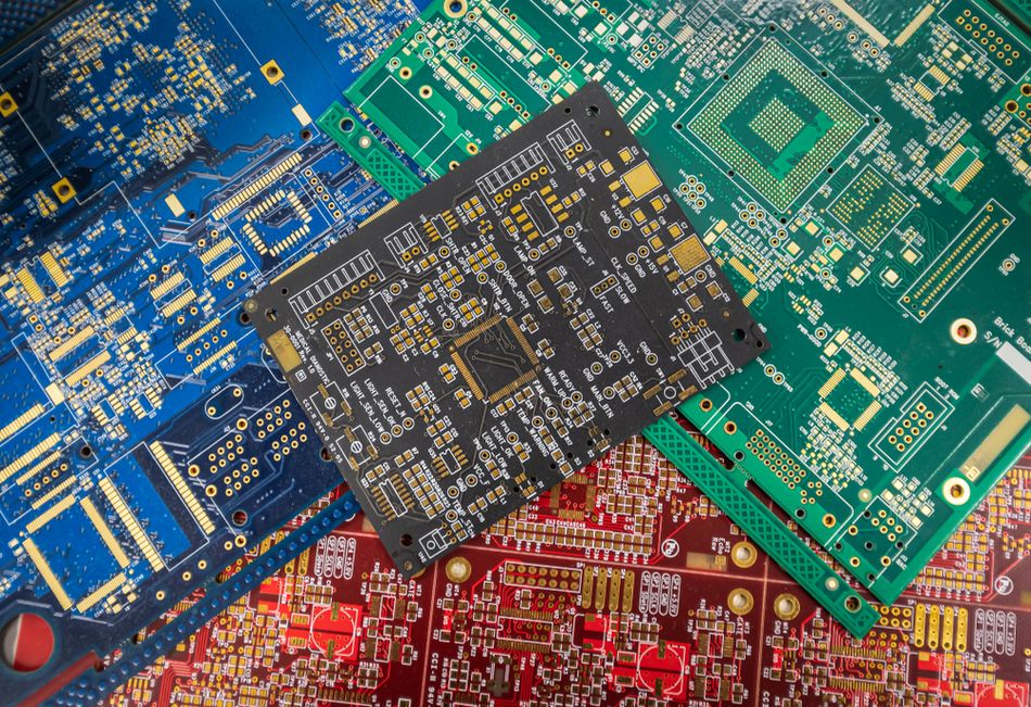
A Printed Circuit Board (PCB) is a flat board made of insulating material with conductive copper pathways etched onto it. These copper traces form the electrical connections between electronic components.
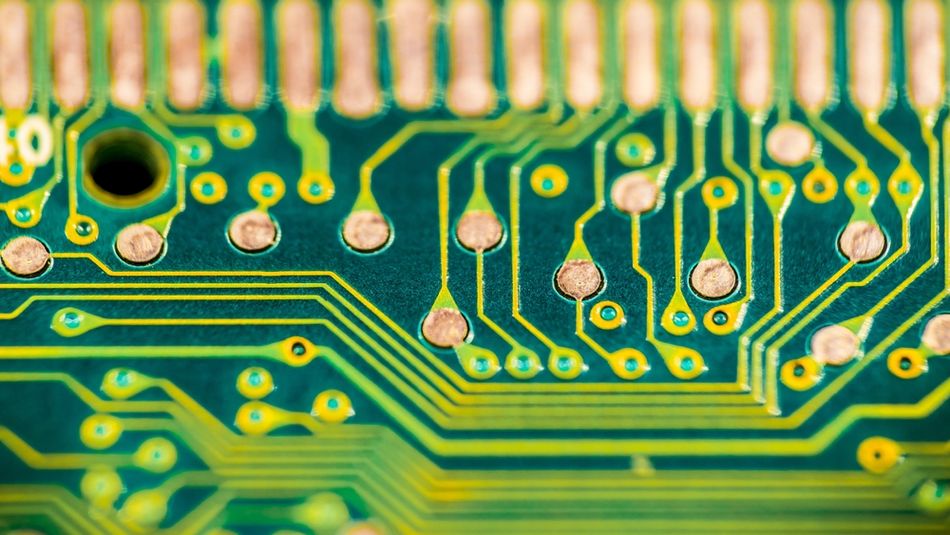
In essence, a PCB is a structure that mechanically supports and electrically connects electronic components into a unified circuit. The PCB itself typically consists of multiple layers: at minimum, a dielectric substrate and one or more copper layers that form circuits. Components will later be attached to this board, but in its bare state, a PCB has no electronic components mounted.
Construction
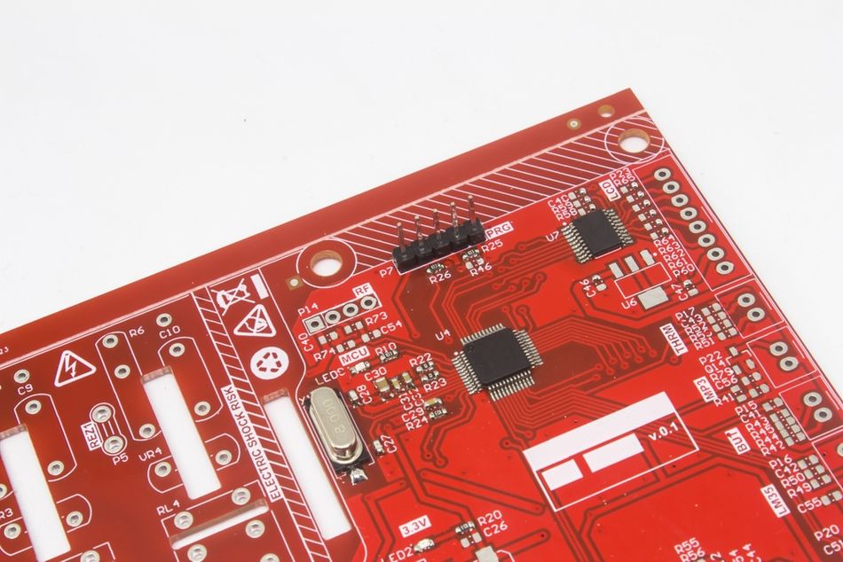
Most PCBs use a rigid fiberglass epoxy substrate material (commonly FR-4 for its flame-retardant properties), though some use flexible plastic film for flexible PCBs. [1] Copper foil is laminated onto the substrate and then selectively etched to create copper traces (wires) that connect component pads. PCBs also include drilled holes – some plated with copper (called vias) – to allow connections between layers or to mount through-hole components. A protective solder mask (often green) is applied to insulate and protect the copper traces, with openings where components will be soldered. White silkscreen labels may be printed to indicate component reference designators or symbols on the board.
Types of PCBs
PCB designs can range from very simple to highly complex, and they come in several types based on structure and application.
Let’s go through their details:
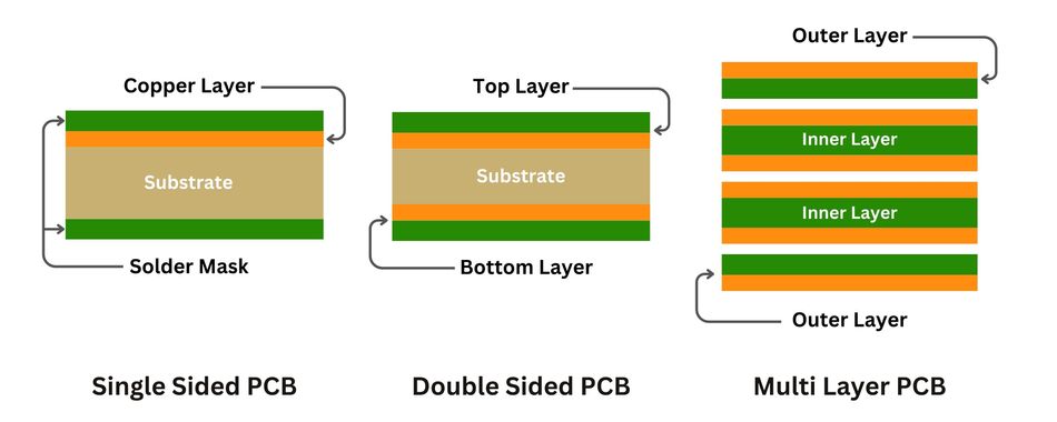
Single-layer PCB (Single-Sided): A PCB with copper traces on only one side of the substrate. Components are typically mounted on the opposite side. Used in simple electronics (e.g., basic gadgets, power supplies).
Double-layer PCB (Double-Sided): Copper layers on both sides of the board, allowing more routing density than single-layer. Vias (through-holes) connect traces between the two sides. Common in moderate complexity circuits (e.g., home appliances, instrumentation).
Multi-layer PCB: A board with three or more copper layers, stacked with insulating layers in between. Vias (through-hole, blind, buried) connect the layers. Multi-layer PCBs enable high-density interconnects for complex circuits and are found in advanced devices like computer motherboards and smartphones (often 4-layer, 6-layer, up to 8+ layers). High-layer-count boards (even 50+ layers) are used in server backplanes or aerospace systems for very complex routing.
Flexible PCB (Flex) and Rigid-Flex: A flex PCB uses a flexible plastic substrate (like Kapton) allowing the board to bend or fold. Rigid-flex boards combine rigid sections and flexible sections in one PCB, often used in compact devices (e.g., foldable phones, and cameras) to save space and weight.
Each type of PCB is chosen based on the application’s needs. For example, a simple toy may use a single-layer PCB, while an advanced GPU card uses a multi-layer PCB with controlled impedance for high-speed signals.
Use Cases
PCBs are the fundamental building blocks of almost all electronic equipment. They appear in everyday consumer electronics (smartphones, laptops, TVs, appliances), industrial machines, automotive electronics, medical devices, aerospace systems, and more.
Essentially, any electronic device with more than a couple of components will have a PCB to hold and interconnect those parts. However, as a bare board, a PCB on its own does nothing until components are added. This is where PCB assembly comes into play, turning a static PCB into an active circuit.
Recommended Reading: Types of Printed Circuit Boards: A Comprehensive Guide
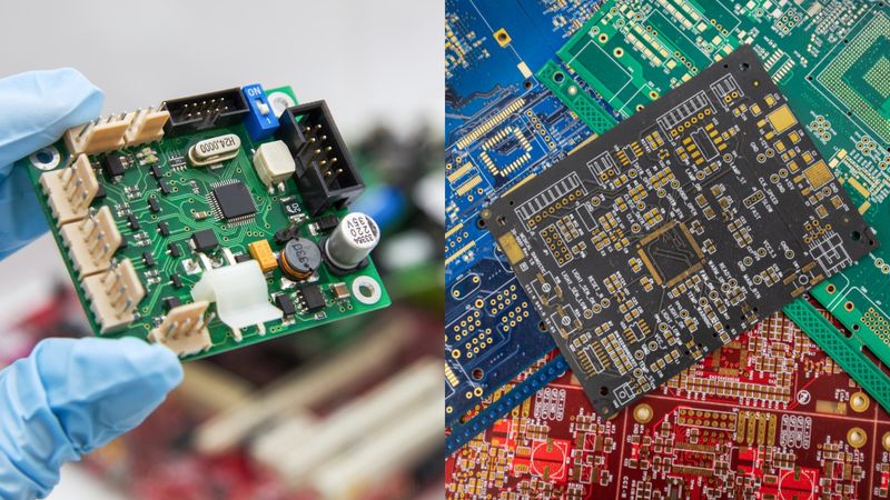
What is a PCBA?
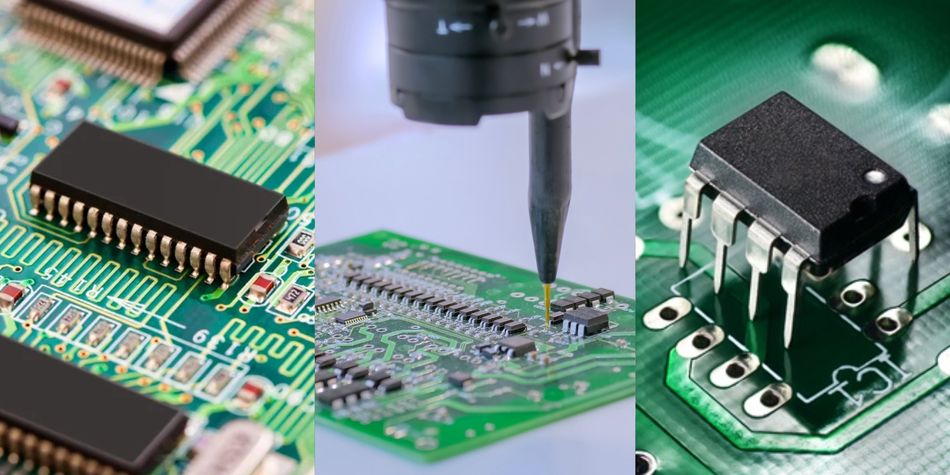
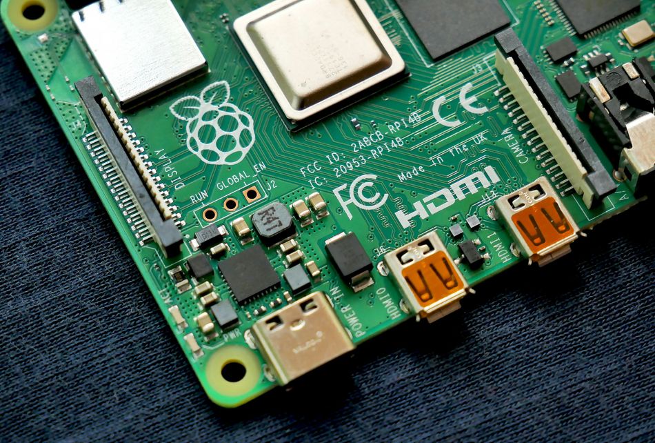
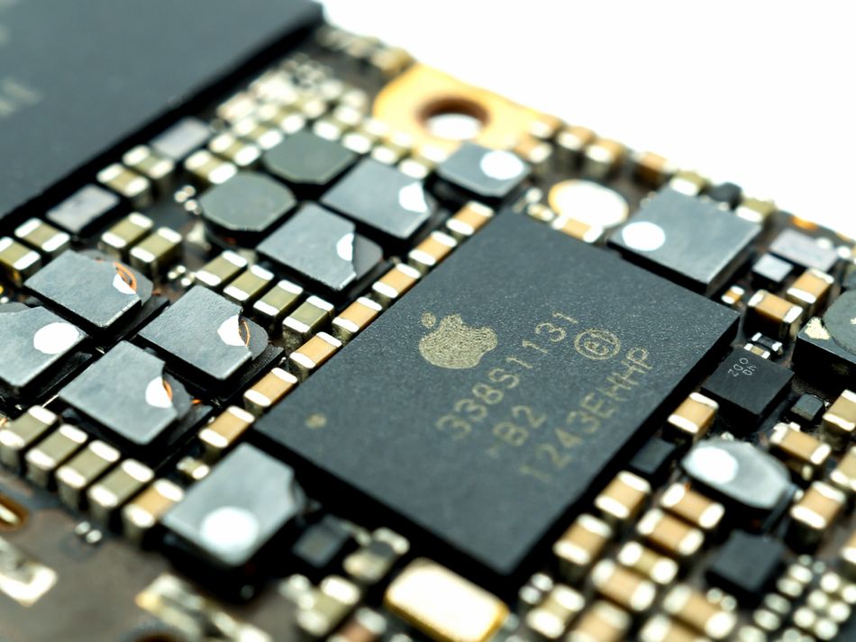
A Printed Circuit Board Assembly (PCBA) is a PCB that has been fully assembled with electronic components, such as resistors, capacitors, integrated circuits (ICs), connectors, and so on. Once a PCB has all the necessary parts mounted and soldered onto it, it becomes a PCBA – a complete circuit board that can perform its intended function. In other words, a PCBA is the finished product of populating a PCB with components, creating a functional electronic circuit.
Assembly Process
The process of going from a blank PCB to a PCBA is called PCB assembly. This involves several steps and can be done using two primary techniques.
Let’s go through their basics:
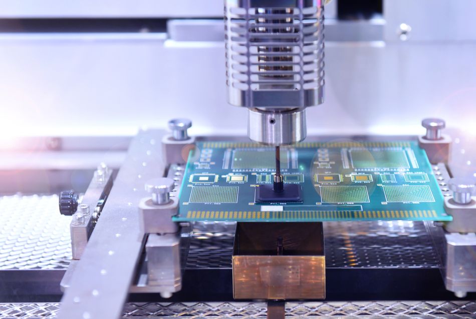
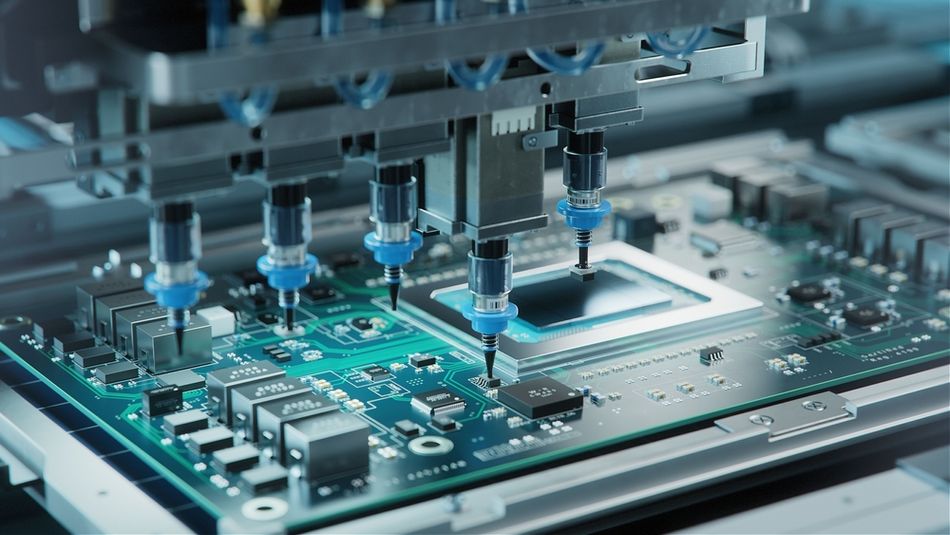
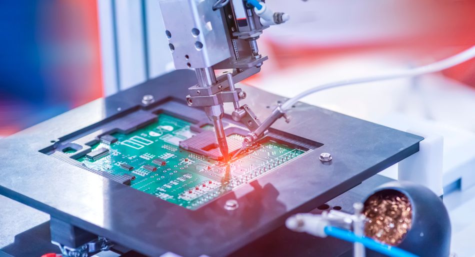
Surface-Mount Technology (SMT): In SMT assembly, components (often called SMDs – Surface Mount Devices) are placed directly onto the surface of the PCB pads. Solder paste (a mixture of solder and flux) is first applied to the component pads on the PCB. Then automated pick-and-place machines place the SMD components onto these pads. The board is passed through a reflow soldering oven, where the solder paste melts and solders the component leads to the pads. SMT is very common in modern electronics because it allows high component density and assembly on both sides of the PCB if needed.
Through-Hole Technology (THT): In through-hole assembly, components with lead wires (like traditional resistors, capacitors, or connectors) are inserted through drilled holes in the PCB. These leads are then soldered, either manually or via a wave soldering machine, to secure them to copper pads on the opposite side. THT provides strong mechanical bonds (useful for connectors or parts that endure mechanical stress) and is sometimes used for reliability in harsh environments. However, it is less dense and often more labor-intensive than SMT.
Mixed Assembly: Many PCBAs use a mix of SMT and through-hole components. For example, most small components (ICs, chips, small resistors) are SMT, while connectors or large capacitors might be through-hole. The assembly process can involve multiple passes to accommodate both methods.
Typical Assembly Steps
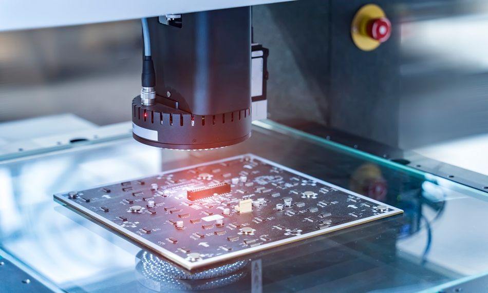
Typical assembly steps include printing solder paste on the PCB pads, placing components, soldering (reflow for SMT, or wave solder for through-hole), followed by inspection and testing. [2] Automated Optical Inspection (AOI) and X-ray inspection (for hidden solder joints like BGA chips) are used to catch soldering defects. Finally, each PCBA may undergo electrical tests such as in-circuit testing (checking each component/node) or functional testing as a whole.
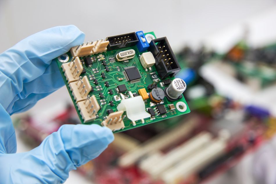
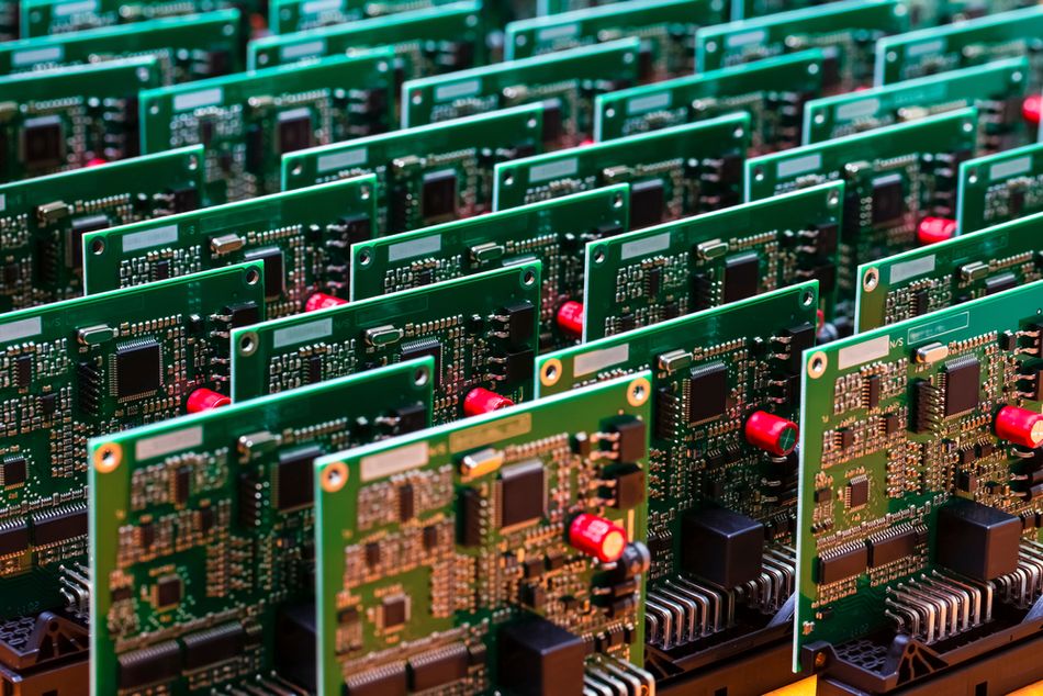
Once assembled, the board is no longer just a PCB – it’s a PCBA ready to be integrated into an electronic device or system. The presence of components means the PCBA can perform tasks: a PCBA might be a power supply module, a computer motherboard, or a sensor interface, depending on what components were assembled and how the circuit is designed.
Significance
The PCBA is what truly powers electronic devices. For example, the PCB inside a smartphone becomes a smartphone motherboard PCBA after all chips (CPU, memory, radio modules) and tiny passive components are soldered on. This PCBA can boot up and operate the phone. Without assembly, the PCB would just be an inert object. In informal usage, people may refer to a PCBA simply as the term PCB once it's in the device, but technically the correct term for a populated board is PCBA (also sometimes called PCA – Printed Circuit Assembly, or CCA – Circuit Card Assembly in industry standards).
Recommended Reading: Through Hole vs Surface Mount: Unveiling the Optimal PCB Assembly Technique
Key Differences Between PCB and PCBA
PCB and PCBA are closely related – in fact, they are sequential stages in the electronics manufacturing process – but they have important differences in definition, design focus, manufacturing, and usage.
Comparison: PCB vs PCBA
Below is a comparison of PCB vs PCBA across key aspects:
| Aspect | PCB (Printed Circuit Board) | PCBA (Printed Circuit Board Assembly) |
| Definition | Bare, unpopulated board providing electrical connections | Populated PCB with electronic components, forming a functional circuit |
| Function | Mechanical support and electrical pathways for components | Performs a specific electronic function |
| Components | None (empty board) | All necessary electronic components (resistors, capacitors, ICs, etc.) |
| Appearance | Flat board with conductive tracks, pads, and holes | Board with various electronic components attached |
| Manufacturing | Etching copper layers onto a substrate; applying solder mask | Placing and soldering components onto the PCB (SMT, through-hole) |
| Testing | Continuity and short testing of copper traces | Comprehensive testing (ICT, functional testing) to ensure proper operation |
| Stage | Foundation/Base | Completed/Functional Circuit |
| Applications | Used in early design stages, prototyping, and circuit validation | Used in final products like smartphones, computers, and industrial electronics |
PCB is the raw, unpopulated board, whereas a PCBA is the realized circuit ready to operate. The PCB is all about the physical design of the circuit pathways, and the PCBA is about the actual functioning circuit with components. A helpful way to remember the distinction is: PCB + Components + Soldering = PCBA. In fact, without a PCB you cannot have a PCBA – the PCB is the first step, and the PCBA builds upon it.
Cost and Lead Time
A bare board PCB can be fabricated relatively quickly and cheaply, especially when using standard PCB materials such as fiberglass or polyimide. However, it remains incomplete until converted into a printed circuit board assembly (PCBA). The transition from PWB vs PCB significantly impacts both cost and lead time due to the addition of conductive traces, circuitry, and components. Assembling a PWB assembly into a functional PCBA involves surface mount technology (SMT) or point-to-point soldering, increasing expenses for components, labor, and testing.
For example, a hobbyist may spend only a few dollars for a small printed wiring board, but integrating copper traces, conductive layers, and components could raise the cost dramatically. Additionally, industries such as high-frequency telecommunications require stringent quality standards set by IPC, further lengthening production timelines. The choice of routing, dielectric properties, and interconnections also affects pricing, making cost optimization a critical aspect of electronic design.
Design Workflow
The design workflow for electronic products clearly distinguishes between PCB and PCBA stages. Engineers initiate the process by meticulously designing the PCB layout using Computer-Aided Design (CAD) tools, often referred to as Electronic Design Automation (EDA) software. [3] This crucial step involves defining the electrical connections and physical arrangement of components on the board. Once the PCB design is finalized, the next phase involves fabrication. This can be achieved through internal manufacturing or by engaging specialized PCB fabrication services.
Subsequently, the choice arises: engineers can either undertake the assembly process themselves, involving the precise soldering of components onto the PCB, or they can opt to outsource this task to a dedicated assembly house. This assembly transforms the bare PCB into a fully populated PCBA.
Recommended Reading: PCB Manufacturing Process: A Comprehensive Guide to Understanding and Mastering the Techniques
Practical Applications and Industry Usage
Both PCBs and PCBAs are essential in the electronics industry, and they ultimately end up in the same applications, but at different stages.
Here we consider how they are used in practice and give examples across various industries:
Prototyping and DIY Projects: During early development or in educational settings, engineers and students often order bare PCBs. This allows them to solder and swap components by hand for testing and debugging. For example, a student designing a custom Arduino shield might print a PCB and then hand-solder components. Bare PCBs are ideal here because they are cheaper and any design changes only waste the board, not assembled parts. It's even easier to rework or modify a PCB during prototyping.
In-House Assembly for Low to Mid Volumes: Many companies or labs with in-house assembly capabilities will purchase PCBs and assemble them internally. For instance, an electronics startup might get 100 bare PCBs made and then have their technicians solder components on-site. This approach gives them control over component sourcing, allows tweaking the assembly process, and can be cost-effective if labor is available and volumes are not too high.
Turnkey Manufacturing: For mass production or when time-to-market is crucial, businesses often opt for turnkey PCBA services – meaning they contract a manufacturer to deliver fully assembled boards. In this case, they directly receive PCBAs that are ready to be integrated into the final product. This is common in consumer electronics and startups without assembly lines; for example, a company designing a fitness tracker will get hundreds of PCBAs built by a contract manufacturer and then simply put them into plastic enclosures. Turnkey PCBAs come with the benefit of professional assembly quality and testing (often with warranties/quality guarantees).
Industry Specific Examples
Now, looking at industry-specific examples, PCBAs (and their underlying PCBs) are ubiquitous.
Here are some real-world application examples:
Consumer Electronics: Smartphones, laptops, TVs, gaming consoles, and appliances all contain one or several PCBAs. For example, a smartphone mainboard is a high-density multi-layer PCBA carrying the processor, memory, radios, and sensors. These devices push PCB technology to have fine traces and many layers, and push PCBA technology to place tiny components (like 0.4 mm pitch BGAs and 01005 size passives) with high precision. [4]
Automotive Electronics: Modern vehicles are full of electronics – engine control units (ECUs), anti-lock brake systems, infotainment systems, sensors, and battery management systems in electric cars. These all use PCBAs. Automotive PCBAs often must endure wide temperature ranges and vibrations, so they may use thicker PCBs or special materials and a mix of SMT and through-hole for reliability. For instance, an airbag control module PCBA will have a robust PCB and secure component soldering to ensure it never fails when needed.
Medical Devices: From small implants like pacemakers to large imaging machines (MRI, ultrasound), medical devices rely on reliable PCBAs. A pacemaker has a tiny PCBA that must work flawlessly for years inside the body – this means strict standards on PCB material (biocompatibility, longevity) and assembly quality. Diagnostic machines have complex boards that handle sensitive analog signals, requiring careful PCB design and shielding, as well as thorough testing of the PCBA for safety.
Industrial & Automation: Factory equipment, robotics, and industrial controllers (PLCs, motor drivers) use PCBAs for control and power electronics. These boards might be designed with heavy copper PCBs for carrying large currents or with conformal coating on the PCBA to protect against dust and moisture in an industrial environment. For example, a motor drive PCBA will have a PCB with thick copper and power transistors soldered on, capable of handling high power.
Telecommunications: Routers, switches, cellular base stations, and other telecom gear contain high-performance PCBAs. These often involve large, multi-layer PCBs with high-speed signal paths and even RF components. The PCBA might include FPGAs, network processors, and memory chips, all assembled with precision. The design and assembly must ensure signal integrity at high frequencies (GHz), so materials and assembly processes are top-notch (e.g., using controlled impedance PCBs and X-ray inspection for BGA solder joints).
Aerospace and Defense: In satellites, aircraft, and military systems, PCBAs must meet extreme reliability standards. PCBs might be made from specialized high-temperature or high-frequency laminates. PCBAs could be enclosed in shielded housings. One example is the avionics in a commercial jet, which include multiple PCBAs for radar, communication, and flight control – each is assembled and then often conformally coated or potted for reliability. The cost here is much less of a concern than absolute reliability and performance.
The role of bare board PCBs in these contexts is usually behind the scenes: PCBs are what engineers design and have manufactured as part of the process of getting to the final PCBA. In summary, you’ll find PCBs being talked about during design and manufacturing, and PCBAs being delivered and integrated into devices. Regardless of the domain – be it a consumer gadget or a spacecraft – the journey goes from PCB design to PCB fabrication to PCBA assembly, and finally to deployment in the field.
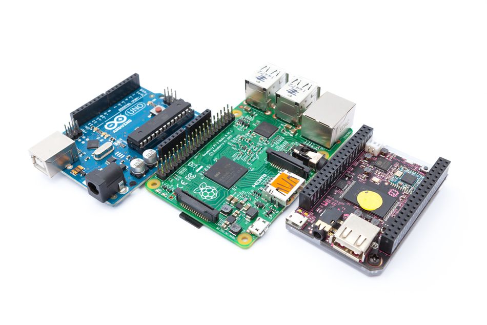
It’s worth noting that with the rise of modular electronics and dev-kits, sometimes hobbyists or engineers will directly use ready-made PCBAs – like an Arduino or a Raspberry Pi which are PCBAs – as components in larger projects. But those PCBAs themselves were manufactured from PCBs internally.
Recommended Reading: Arduino vs Raspberry Pi: Choosing the Right Platform for Your Next Project
Manufacturing and Cost Considerations
When comparing PCBA vs PCB from a manufacturing and cost perspective, several factors come into play: fabrication processes, assembly steps, complexity, and economies of scale. Both PCB fabrication and PCB assembly have their own cost structures and challenges, so understanding these can help in planning a project or product rollout.
PCB Fabrication Costs and Challenges
The cost of producing bare PCBs depends on a few key factors – board size, number of layers, complexity of the circuit (trace density, minimum trace width/spacing), material, and quantity. A simple two-layer PCB on FR-4 material is relatively inexpensive especially when ordered in bulk. However, as you increase the layer count or require special features (e.g., very fine traces, controlled impedance, high-temperature materials, or flexible design substrates), the fabrication process becomes more complex and costly. For instance, a 6-layer PCB will cost more than a 2-layer PCB due to additional lamination steps and materials. Likewise, adding features like blind/buried vias or using exotic RF substrates (for high-frequency circuits) raises costs.
Manufacturing challenges for PCBs often include ensuring the alignment of layers, drilling many precise via holes, and preventing defects like delamination or etching faults. For mass production of PCBs, panelization is used (multiple boards per panel) to optimize fabrication and reduce cost per board. Generally, producing bare PCBs is faster and cheaper than full assemblies because it’s a single streamlined process (just board fabrication). Turnaround for a PCB can be as quick as a couple of days for prototypes. And companies often take advantage of low-cost PCB manufacturers globally for this stage.
PCBA Manufacturing Costs and Challenges
The cost of PCBA builds upon the cost of the PCB itself and then adds several layers of additional cost: component procurement, assembly labor (or machine operation), soldering materials, and testing.
Each of these can be significant:
Component costs: These can vary widely. Common resistors or capacitors cost only fractions of a cent, but specialized ICs or connectors could be dollars or tens of dollars each. If your design uses many components, the sum cost of all parts (often called the Bill of Materials or BOM cost) can dominate. Also, component availability is a factor – if a component is hard to source, it might drive costs up or delay production.
Assembly labor and setup: If using a contract manufacturer, there is usually an initial setup cost for assembly (programming pick-and-place machines, making solder paste stencils, etc.). This can be a few hundred dollars or more, which is amortized over the production volume. This means small runs of PCBAs can be disproportionately expensive per unit because you still pay for the setup. In contrast, hand-assembling one or two boards yourself avoids that cost, but is time-consuming and not feasible for fine-pitch or high-volume. In mass production, automated assembly is a must, and the cost per board goes down as volume increases (after recouping setup costs).
Yield and rework: Not every assembled board will pass testing on the first go. Complex PCBAs might have some yield loss (boards that need rework or scrap due to soldering defects or component failures). Manufacturers factor this into cost. Designing for manufacturability (good PCB layout, proper land patterns, penalization for assembly, etc.) helps keep yield high and costs down.
Testing and QA: Especially for complex or high-reliability products, each PCBA might undergo an ICT (in-circuit test) or functional test. [5] Setting up test fixtures and writing test procedures adds to the cost. However, it’s crucial to ensure each PCBA works as intended, particularly in industries like automotive or aerospace.
In general, a PCBA is more expensive and time-consuming to produce than a PCB because of the added steps and resources. For example, even if a bare PCB costs $5 to make, once you add $15 worth of components and $10 of assembly cost, the PCBA might cost $30 (these numbers are illustrative). Producing a PCBA also typically extends lead time: you need to get the PCB made, source components (which might have lead times of their own), and then perform assembly and testing. It’s not uncommon for a PCBA order to take several weeks from start to finish, whereas bare PCBs might be delivered in a week or less.
Mass Production Considerations
In large-scale production (hundreds of thousands of units), cost efficiencies become critical. PCBs are often produced in large panels and bulk to minimize cost per board. Assembly lines are optimized for throughput – high-speed pick-and-place machines can place tens of thousands of components per hour. Still, challenges exist: component supply must be reliable (parts shortages can halt a line), and any design issue discovered late can be costly if many PCBAs are already produced. Manufacturers may do a pilot run (small batch of PCBAs) to verify the process before ramping to full production.
Another consideration is that some companies separate PCB fabrication and assembly across different specialized vendors (especially if they require very high-end PCBs from a particular fab, but have an in-house assembly). Others use one vendor for a turnkey solution. There is no one-size-fits-all – decisions are made based on cost, capability, and logistical convenience.
Design Complexities and Impact on Manufacturing
The complexity of the design can affect both PCB and PCBA manufacturing. For PCBs, a high-density design might push fabrication limits (like very thin traces or microvias) which can increase the chance of defects and fabrication difficulty. For PCBAs, having many fine-pitch components (like 0.5 mm or smaller pitched ICs, BGA chips, or components on both sides of the board) means the assembly process has to be very well calibrated. The more complex the PCBA (component count, packaging types, etc.), the more careful the assembly process must be to avoid issues like tombstoning of tiny parts, misaligned BGA, etc. Design for Assembly (DFA) is an important practice: for example, ensuring components are not placed too close to board edges (so the machine can grip the board), or all polarized components have clear markings to avoid placement errors, etc. Likewise, Design for Manufacturing (DFM) for PCBs might involve ensuring adequate clearances, avoiding acute angles in copper that might etch poorly, and so on.
In terms of cost, design choices can heavily influence it: choosing an expensive component vs a cheaper equivalent, or deciding to use a 4-layer PCB vs a 2-layer PCB, will impact the bottom line. Engineers must balance performance requirements with cost constraints. Often during the prototyping phase, one might overspent or not worry about cost too much; but for the final product that will be mass-produced, optimizing the design for cost (without sacrificing quality) is a key engineering challenge.
In summary, PCB is cheaper and simpler to make, but it’s only the skeleton. A PCBA is the full body, requiring more work and cost but delivering functionality. When planning a project, consider the trade-off – for instance, if you are in early design, you might just order PCBs and solder a few critical components yourself to test. This saves you from paying for full assembly when you know you might change things.
However, when you need dozens or more boards or have very small components, investing in professional PCB assembly becomes worthwhile. Always weigh factors like time, budget, volume, and in-house capability. Sometimes a hybrid approach is used: assemble critical or difficult parts in a factory and hand-solder some simple components yourself to save cost – it all depends on the scenario.
Recommended Reading: Design for Manufacturing (DFM): The Ultimate Guide to Streamlining Product Development and Reducing Costs
The Evolution of PCB and PWB
In the early days of electronics, Printed Wiring Boards (PWB) were widely used as the foundation for circuitry, enabling reliable point-to-point connections in circuit design. Over time, the term PWB evolved, and the industry adopted the abbreviation PCB to distinguish between the bare board and a printed circuit board assembly (PCBA), which includes mounted components. While PWB vs PCB remains a relevant distinction, particularly in regions like Japan, modern electronics favor multilayer boards with conductive layers for improved performance.
The transition to surface mount technology (SMT) and advanced routing techniques have further optimized interconnections, making printed wiring assembly (PWA) more efficient. Materials like fibreglass, polyimide, and non-conductive substrates enhance durability, while conductive traces such as copper traces improve signal integrity, especially in high-frequency applications. Historically, polychlorinated biphenyls were used in certain PCB manufacturing processes but were later phased out due to environmental concerns. Organizations like IPC set standards for PWB assembly, ensuring consistency in electronic design and prototyping across industries.
Recommended Reading: PWB vs PCB: Differences and Similarities
Conclusion
PCB vs PCBA represents the journey from an empty circuit board to a fully functional electronic assembly. A PCB (Printed Circuit Board) is the foundational hardware that provides the wiring and structure for circuits, while a PCBA (Printed Circuit Board Assembly) is that board brought to life with components. For digital design engineers and hardware enthusiasts, understanding the difference is more than semantics – it’s about recognizing the different phases of design and production, each with its own challenges and considerations.
Looking ahead, the worlds of PCB design and PCB assembly are continuously evolving. PCB technology is advancing (with innovations like HDI – High Density Interconnect boards, flexible hybrid electronics, and even 3D printed electronics), and assembly techniques are becoming more automated and precise (with robotics and AI for inspection). These advancements mean that tomorrow’s engineers need to be versed in both layout design and assembly considerations more than ever. Concepts like design for manufacturing and assembly (DFM/DFA) will play an even larger role in ensuring that a PCB design can be smoothly turned into a reliable PCBA.
Frequently Asked Questions (FAQ)
1. Are PCB and PCBA the same thing?
A. No, a PCB (Printed Circuit Board) and a PCBA (Printed Circuit Board Assembly) are not the same, though the terms are related. A PCB refers to a bare board, which has only copper traces and no components. A PCBA refers to the board after all the components have been assembled onto it. In other words, PCBA = PCB + components. Think of the PCB as an empty foundation and the PCBA as the completed building.
2. What does a PCBA include that a PCB doesn’t?
A. PCBA includes all the electronic components mounted to the board, whereas a PCB has no components. The PCB provides the wiring and physical support; the PCBA has the resistors, capacitors, chips, connectors, etc., soldered in place. Because of this, a PCBA can perform a function (blink an LED, compute data, etc.), while a PCB by itself cannot do anything until parts are added.
3. Why is a PCBA more expensive than a PCB?
A. PCBA is more expensive because it encompasses additional materials and work. The cost of a PCB covers the raw board fabrication only. The cost of a PCBA includes the PCB itself plus the cost of all the electronic components and the assembly process (soldering, machine setup, labor, inspection, and testing). As a result, PCBAs have higher costs and typically longer lead times than PCBs. However, the PCBA delivers a finished, functional product, whereas with a PCB alone you’d still have to spend time and money to assemble it.
4. When should I order just PCBs vs. fully assembled PCBAs?
A. It depends on your project needs and capabilities. If you are in the prototyping or development stage and have the ability to solder components yourself, ordering bare PCBs can be more economical and faster for making quick changes. This is common for hobbyists or early hardware startups – get 5-10 PCBs made, then hand-solder or partially assemble them to test the design. On the other hand, if you need a finished product or have a larger batch to produce, it’s usually better to order PCBAs.
5. Can I assemble components on a PCB by myself?
A. Yes, you can assemble components on a PCB yourself if you have the necessary tools and skills. You’ll typically need a soldering iron (or reflow setup for SMT), solder, tweezers, maybe a microscope for very small parts, and patience to place components correctly. THT components are easier for beginners (you just solder the leads), while SMT parts can be trickier but are doable with practice – especially larger package sizes.
6. Do all PCB manufacturers also offer assembly (PCBA) services?
A. Not all PCB fabricators offer assembly, but many do or have partners that do. There are dedicated PCB manufacturers whose main service is making bare boards; if you send them Gerber files, they send you PCBs. Separately, there are contract manufacturers focused on assembly – you send them the PCB design and BOM, and they source parts and assemble boards (sometimes you provide the PCBs to them, or they get them made for you).
References
[1] Wevolver. FR4: Understanding the Material and Its Applications in PCB Design [Cited 2025 January 23] Available at: Link
[2] Cadence. PCB Assembly and Soldering Techniques [Cited 2025 January 23] Available at: Link
[3] Altium. PCB Design Process: The EDA Design Approach [Cited 2025 January 23] Available at: Link
[4] Viasion. Key Components of a PCB: Layers, Traces, and Pads Explained [Cited 2025 January 23] Available at: Link
[5] Acculogic. Introduction to In-Circuit Testing (ICT) [Cited 2025 January 23] Available at: Link
Table of Contents
IntroductionWhat is a PCB?ConstructionTypes of PCBsUse Cases What is a PCBA?Assembly ProcessTypical Assembly Steps SignificanceKey Differences Between PCB and PCBAComparison: PCB vs PCBACost and Lead TimeDesign WorkflowPractical Applications and Industry UsageIndustry Specific ExamplesManufacturing and Cost ConsiderationsPCB Fabrication Costs and ChallengesPCBA Manufacturing Costs and ChallengesMass Production ConsiderationsDesign Complexities and Impact on Manufacturing The Evolution of PCB and PWBConclusionFrequently Asked Questions (FAQ)References