VSS vs VDD: Understanding Power Rails in Electronic Circuit Design
VSS and VDD are crucial power rails in electronics—VDD is the positive supply (often for MOSFET drains), while VSS is ground or negative reference. Learn their roles in CMOS/BJT circuits, their impact on analog/digital design, and PCB layout best practices.

09 Apr, 2025. 23 minutes read
Introduction
In electronic circuit design, distinguishing between VSS and VDD is essential for anyone working with digital or analog hardware. These power rail notations appear in schematics and datasheets, defining the voltage references that drive integrated circuits (ICs). Engineers and students often encounter VDD, VSS, VCC, VEE, and GND, leading to questions about their roles and differences.
VDD and VSS originate from MOSFET-based circuits, where VDD represents the drain supply voltage (typically positive), and VSS refers to the source voltage (often ground). In CMOS logic circuits, VDD is the supply for the PMOS transistors, while VSS serves as the reference for the NMOS transistors. This convention differs from bipolar junction transistor (BJT) circuits, where VCC and VEE are commonly used instead.
Proper design and layout of power rails are crucial for circuit stability and noise immunity. Power integrity, ground planes, decoupling capacitor placement, and multi-voltage domain management influence performance. Modern systems frequently incorporate multiple power domains, such as core voltage vs. I/O voltage, making a clear understanding of VDD and VSS even more critical.
Additionally, understanding the relationship between VDD, VSS, and other power rails is crucial for preventing ground loops, voltage drops, and unintended coupling effects, which can degrade circuit performance and signal integrity.
Recommended reading: Understanding NPN vs PNP Transistors: A Comprehensive Guide
What Are VSS and VDD? (Theoretical Concepts)
VDD and VSS are power rail designations in electronic circuits, particularly in MOSFET-based devices. These terms originate from field-effect transistor (FET) terminology and have become standard in modern integrated circuits (ICs).
VDD: Voltage at the Drain
In n-channel MOSFETs, the drain is connected to the positive supply voltage. Thus, VDD refers to the positive power rail supplying voltage to the circuit's MOSFET drains. In practical applications, VDD is the main supply voltage for an IC, typically at +5V, +3.3V, or other levels depending on the system requirements. When a datasheet states “apply power to VDD,” it means connecting the positive supply voltage to the pin labeled VDD.
VSS: Voltage at the Source
In contrast, the source of an n-channel MOSFET is usually connected to the negative supply rail or ground. VSS represents the 0V reference point in most circuits, serving as the return path for current flowing from VDD. It acts as the common ground reference for voltage measurements and signal integrity. In schematics, VSS is often interchangeable with GND (ground) and is frequently represented by the standard ground symbol (⏚). Many datasheets explicitly state “VSS = 0V” to reinforce this convention.
VDD and VSS in CMOS Circuits
In CMOS (Complementary MOS) technology, both p-channel and n-channel MOSFETs are used:
P-channel MOSFETs have their sources connected to VDD (positive supply).
N-channel MOSFETs have their sources connected to VSS (ground).
Although both supply rails connect to transistor sources, the terms VDD and VSS remain standard for denoting power rails in CMOS circuits.
Why the Double Letters (DD and SS)?
The use of double letters (DD and SS) is a historical convention, mainly for clarity in circuit schematics:
VDD and VSS distinguish power supply nodes from standard signal nodes.
Single-letter notations (e.g., V_D) often denote instantaneous voltage at a node, while double-letter notations (e.g., V_DD) indicate a constant DC supply voltage.
Recommended reading: Vdd vs Vss: Key Technical Differences and Implications in Electronics
VDD and VSS in CMOS Logic and Other Families
Modern digital integrated circuits are often built with CMOS technology (Complementary Metal-Oxide-Semiconductor). In a CMOS inverter (the simplest CMOS logic gate), you have a p-channel MOSFET on top and an n-channel MOSFET at the bottom. The p-channel’s source is tied to VDD, and the n-channel’s source is tied to VSS (ground). The drains of both transistors join together to form the output. When the input to the inverter is low (0 V), the p-channel conducts, connecting the output to VDD (logic high). When the input is high (VDD), the n-channel conducts, pulling the output down to VSS (logic low).
In both cases, one of the transistors connects the output node to either VDD or VSS, thus producing a digital ‘1’ or ‘0’ corresponding to the supply levels. Throughout this operation, VDD provides the logic “1” voltage level, and VSS provides the logic “0” level (ground). It’s important to realize that CMOS circuits use both VDD and VSS extensively as references. The noise margins, switching thresholds, and output voltage levels in CMOS are all defined relative to these rails. For example, a CMOS logic gate’s high output will be approximately VDD, and its low output will be VSS (0 V). The entire logic family’s behavior assumes that one stable supply (VDD) defines the high logic level and the stable reference (VSS) defines the low logic level. This is why maintaining stable VDD and a low-impedance VSS (ground) is so critical in digital systems – any fluctuation in these “anchor” voltages can cause logic errors.
Other logic families have their historical naming conventions:
TTL (Transistor-Transistor Logic) and many bipolar logic families typically used VCC for the positive supply and GND for ground. VCC stands for Voltage at the Collector, reflecting that in an NPN bipolar transistor, the collector is tied to the positive rail. TTL chips (e.g., 7400-series ICs) often have pins labeled VCC (usually +5 V) and GND (0 V).
ECL (Emitter Coupled Logic) might use VCC for ground and VEE for a negative supply (since ECL often uses a negative rail for the emitter network).
Analog op-amps and amplifiers often use V+ and V- or VCC and VEE to denote the positive and negative supply rails, since analog circuits commonly have dual supplies (e.g., +12 V and -12 V, where ground is in the middle). For instance, in an op-amp datasheet, VCC might be +5 V and VEE -5 V, or they might simply say V+ = 5 V, V- = 0 V for a single-supply op amp.
Recommended reading: Understanding Transistors: What They Are and How They Work
In many modern microcontrollers and digital ICs, whether they use CMOS internally or not, you will see either VDD/VSS or VCC/GND used almost interchangeably. Manufacturers choose the nomenclature based on the internal transistor technology or simply tradition. For example:
Microcontrollers from Microchip (PIC series) and many other CMOS chips use VDD for the supply and VSS for ground. On a PIC16F877A microcontroller, you’ll find multiple VDD and VSS pins to connect to 5 V and ground, respectively.
Microcontrollers from Atmel (AVR series like ATmega328) often label the digital supply as VCC and ground as GND, even though internally they are CMOS. They might reserve VDD for an analog supply in some cases, or simply stick to the VCC term out of convention. On an Arduino (which uses an ATmega328P), the 5 V pin is often referred to as VCC in the microcontroller’s datasheet, and ground is GND.
The key point is: VDD vs VCC – both typically mean the primary positive supply voltage for the chip, just in different terminology. Likewise, VSS vs GND vs VEE usually means the ground or negative reference. It’s crucial to check the datasheet of the component you are using to see which convention is followed. Often, a datasheet will explicitly state something like “VDD (Supply Voltage) must be 2.7 V to 5.5 V” or “Connect all VSS pins to ground.” Once you map the nomenclature, the electrical role is clear.
Common Power Rail Labels and Their Meanings
Label | Meaning (Expanded) | Typical Use Case / Context |
VDD | Voltage at the Drain | + Supply in MOSFET/CMOS circuits (e.g., microcontrollers, memory, digital ICs). Provides power for logic ‘1’. |
VSS | Voltage at the Source | Ground or negative supply in MOSFET/CMOS circuits. Acts as the common reference (0V) for signals. |
VCC | Voltage at the Collector | + Supply in BJT circuits (e.g., TTL logic, some analog circuits). Often +5V in TTL. Synonymous with VDD in many modern digital ICs. |
VEE | Voltage at the Emitter | Ground or negative supply in BJT circuits. Often, 0V or a negative rail is used in NPN transistor circuits. (For PNP transistors, signs are reversed.) |
GND | Ground (Zero reference) | Common return path for current, 0V reference in circuits. Used for safety, often tied to chassis ground in EMI-sensitive designs. |
V+ / V- | Positive / Negative supply | Used in analog circuits (e.g., op-amps, amplifiers). Example: V+ = +12V, V- = -12V in dual-supply configurations. In single-supply circuits, V may be 0V (ground). |
VBB | Voltage at the Base | Bias supply for BJT base circuits. Less common in digital, more prevalent in analog biasing networks. |
VSS vs VDD in Analog vs Digital Design
While VDD and VSS are terms most often encountered in digital logic circuits (like microprocessors, memory chips, digital ICs, etc.), they also appear in analog and mixed-signal devices. However, analog design can sometimes have more complex power rail requirements:
Digital Designs (Single-Supply): The vast majority of digital circuits today run off a single positive supply rail (VDD) and ground (VSS). Negative voltages are rarely used in pure digital logic. For example, a microcontroller might run at VDD = 3.3 V and VSS = 0 V. All internal transistors operate between these bounds, and all I/O signals are referenced to VSS (ground). In these systems, ground is the most negative voltage available. Everything from logic levels to interface standards (like TTL, CMOS, LVCMOS, etc.) is defined by that single supply. This simplifies design: one rail and ground. However, the simplicity comes with the need for careful decoupling and ground management because any noise on VDD or VSS directly affects logic levels.
Analog Designs (Dual-Supply or Single-Supply): Analog circuits (such as operational amplifiers, ADCs, DACs) often need to handle signals that swing positive and negative relative to ground (especially for AC signals like audio). Historically, analog systems might use a dual power supply, e.g., +12 V (often labeled VCC) and -12 V (often labeled VEE), with ground in the middle as a 0 V reference. In such cases, you might not see VDD/VSS on the schematic because the designer used analog notation (V+, V-). However, if the analog IC is CMOS internally (many modern op-amps and ADCs are CMOS), the datasheet might still refer to its positive supply as VDD and negative supply as VSS (or ground). For instance, a CMOS op-amp that can run off ±5 V might label its pins VDD and VSS, where VDD = +5 V and VSS = -5 V. It’s crucial to realize here that VSS is not 0 V but -5 V relative to ground. The ground is midway. This is a bit of a twist: in analog CMOS, sometimes VSS means the negative supply rail, which could be below ground potential, whereas in digital CMOS, VSS is usually ground (the most negative rail available).
In single-supply analog designs (which are very common now to interface with digital), the analog IC might have VDD = e.g., +5 V and VSS = 0 V (ground), just like a digital IC. The difference is that the analog signals are often biased around mid-supply or use techniques to handle input signals near ground. Some ADCs and DACs have separate analog ground (often labeled AVSS) and analog supply (AVDD) pins in addition to the digital supply (DVDD) and digital ground (DVSS). This segregation is done to prevent digital switching noise from contaminating analog measurements.Mixed-Signal Systems: In microcontrollers and system-on-chip (SoC) designs that incorporate both analog and digital components, you may encounter distinct power rail designations, such as AVDD/AVSS for analog supply and ground, and DVDD/DVSS for digital supply and ground. While these rails often originate from the same primary voltage source (e.g., 3.3V) and ground on the PCB, they are kept separate in layout and routing to minimize noise and improve performance. Proper connection of these power domains is crucial. The standard practice is to tie all grounds together at a single point to prevent ground loops and ensure signal integrity. Additionally, adequate decoupling capacitors should be placed between each supply pair to reduce power fluctuations and noise coupling between analog and digital sections. For instance, some Microchip PIC microcontrollers include dedicated analog VDD (AVDD) and analog VSS (AVSS) pins specifically for their analog peripherals. Even if these pins are internally linked to the main power rails, they must still be explicitly connected to the board’s supply and ground to maintain a clean, stable voltage reference for analog circuits. Neglecting this can lead to degraded analog performance due to interference from digital switching noise.
Always consider whether a chip operates on a single or dual supply. In dual-supply analog circuits, VSS typically serves as the negative supply, with ground being either a separate reference point or tied to one of the rails in single-supply mode. In single-supply analog or digital circuits, VSS is generally ground (0V). Effective ground management is crucial—analog designs often use a star grounding or single reference point to minimize noise, while digital circuits rely on a solid ground plane (VSS plane) to ensure proper current return. In both cases, VSS should be a low-impedance node, as any voltage drop across ground can introduce errors, causing hum or offset in analog circuits and logic errors or clock jitter in digital systems.
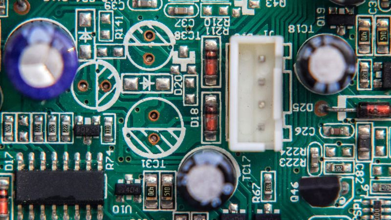
PCB Design Considerations for VDD and VSS
Designing a PCB with good power distribution involves much more than just wiring the VDD pin to a voltage regulator and the VSS pin to a ground symbol. Here are critical considerations to ensure that VDD and VSS truly behave like ideal power rails (stable DC for VDD, solid reference for VSS):
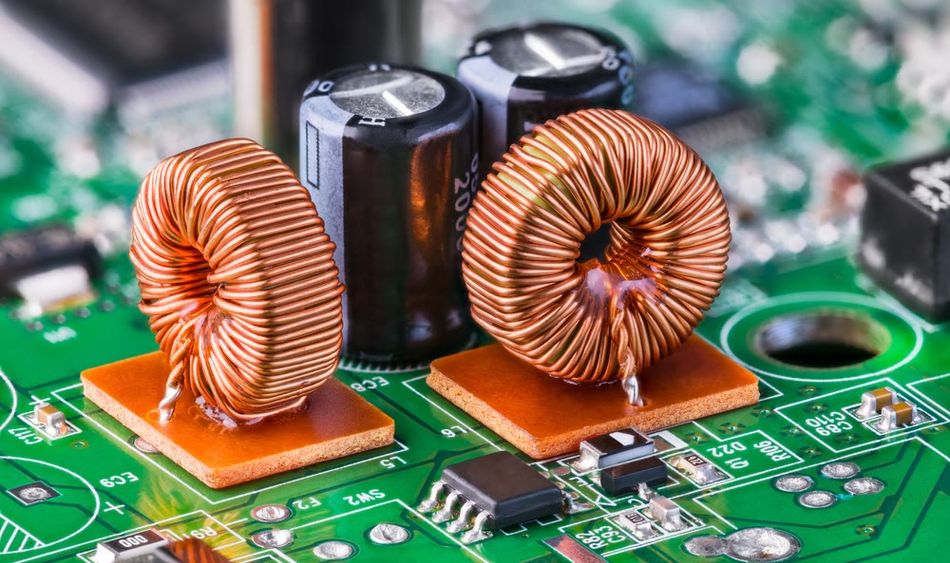
Ground Planes and Power Planes
On any high-speed or complex PCB, you will typically dedicate one or more layers to a ground plane (a continuous copper area connected to VSS) and sometimes a power plane (continuous area for VDD or other supply voltages). These planes serve multiple purposes:
They provide a low impedance path for current flow. The ground plane, in particular, allows return currents from all components to find their way back to the source with minimal resistance and inductance. A low impedance VSS means that when many devices switch simultaneously, the ground voltage at different points on the board stays uniform (preventing what’s known as “ground bounce”).
Power planes (for VDD) help distribute the supply evenly across the board and reduce voltage drop. Instead of routing a thin trace that might have significant resistance, a plane can carry large currents with negligible voltage drop across the board.
A pair of closely spaced power and ground planes in a PCB acts as a large parallel plate decoupling capacitor spread over the board. This is often beneficial at high frequencies – the inter-plane capacitance can help stabilize the supply and shunt high-frequency noise. For example, a PCB with a ground plane directly adjacent to a 3.3 V VDD plane can provide a few tens of pF of capacitance per square centimeter, which helps smooth out transients.
Ground planes also serve as reference planes for signal traces, maintaining signal integrity. Any signal trace that runs above a ground plane has a controlled impedance and a defined return path immediately beneath it (the return current will flow on the ground plane right under the trace due to electromagnetic coupling). This is critical for high-speed design. If you didn’t have a ground plane, return currents would have to find some other path, possibly creating large loops that radiate noise or pick up interference.
In practice, good PCB designs tie all VSS points to a common ground plane. For instance, all the VSS pins of ICs, connectors, etc., are connected through vias to the solid ground layer. This ensures minimal difference in ground potential across the board. Likewise, VDD pins might connect to a power plane or a thick trace that acts like a pseudo-plane. Ground planes dramatically reduce noise and EMI by providing a low-impedance return path. They also help with thermal dissipation and make the layout easier (since you don’t need to route a ground net to every component; they all just via down to the plane).
One must be cautious with multiple ground planes or split ground planes. In mixed-signal designs, you might be tempted to have an “analog ground” plane separate from a “digital ground” plane to isolate noise. This can work if and only if they are connected at a single point (typically near the ADC or the power supply entry) to avoid differential ground voltages. Many ADC/DAC datasheets give guidelines on how to join analog and digital grounds (AGND and DGND). A rule of thumb is to keep analog return currents flowing in an analog ground region and digital returns in a digital ground region, meeting at one node (star ground). That single node could be a bridge or a zero-ohm resistor, or just a common ground point at the power supply. If you completely isolate grounds without a connection, your circuit has no defined reference between analog and digital sections, which can cause erratic behavior or unsafe conditions.
Decoupling Capacitors (Bypass Capacitors)
If you’ve looked at almost any digital or analog circuit schematic, you’ll notice small value capacitors (like 0.1 µF ceramics) placed between the power pins of ICs and ground. These are decoupling capacitors (also called bypass capacitors). Their purpose is to locally stabilize VDD and VSS for each IC.
When a digital IC (like a microprocessor or FPGA) switches its internal transistors, it can cause rapid bursts of current demand from VDD to VSS. The inductance and resistance of the power supply path mean the VDD pin might momentarily dip or the VSS pin might momentarily rise (ground bounce) in response to a fast transient. A decoupling capacitor acts as a tiny battery right at the IC’s pins that can supply the instantaneous current and then recharge slowly from the main supply. By doing so, it filters out voltage spikes and dips, preventing them from propagating across the board.
Best practices for decoupling:
Place a decoupling capacitor as close as possible to each VDD pin–VSS pin pair on an IC. Ideally, the capacitor should be next to the IC’s pins, with a via to ground plane very nearby, minimizing the loop area formed by the VDD->Capacitor->VSS loop. The smaller this loop, the higher the effective frequency the capacitor can decouple (because of lower loop inductance).
Use the typical value of 0.1 µF (100 nF) for high-frequency decoupling, and often a larger capacitor (4.7 µF or 10 µF tantalum or ceramic) somewhere nearby for lower-frequency bulk decoupling. The smaller cap handles fast transients, the larger cap handles slower variations, and keeps the DC level steady.
One capacitor per power pin is a good rule for digital ICs. If a microcontroller has two VDD pins and two VSS pins, it should have at least two decoupling caps (one for each pair). Sharing capacitors between ICs or pins can be less effective, especially if the pins are physically far apart.
Ensure the capacitor’s leads or vias connect one side directly to the VDD pin trace and the other directly to the ground plane (VSS) with minimal length. Often designers will put a via from the capacitor pad straight down into the ground plane right next to the IC pin via. This way, the current loop is essentially the capacitor pad distance.
For very high-speed circuits, special capacitor placements (like directly under BGA chips, on the opposite side of the PCB, or even embedded capacitance in the PCB layers) are used. But for most cases, adjacent placement on the same side is sufficient.
Noise Management and Signal Integrity
Even with good planes and decoupling, designers must be aware of how VDD and VSS interact when many signals are switching:
Ground Bounce: When multiple outputs of an IC switch from low to high or high to low simultaneously, a large surge of current flows through the VSS (ground) network momentarily. This can cause a transient rise in the local ground potential (i.e., the ground at the chip is not exactly 0 V during that split nanosecond). Ground bounce can cause a chip’s internal logic reference to shift, potentially causing false triggering. The preventative measures are exactly what we discussed: multiple ground pins, ground planes, decoupling caps, and sometimes slowing the output edge rates or not switching too many lines at once. Some FPGAs and microcontrollers have several VSS pins precisely to give ground currents multiple paths (reducing inductance).
Power Supply Noise and EMI: Fast edges on current draw can propagate through VDD/VSS and radiate as electromagnetic interference. A solid plane acts as a return current shield to reduce EMI. Decoupling caps localize the currents. Additionally, sometimes small series resistors or ferrite beads are used in series with the VDD line to an IC to filter high-frequency noise (this creates an RC or LC filter with the decoupling cap). In high-frequency designs, one might also employ power supply ferrites and partition power domains to isolate noisy sections from sensitive sections.
Analog ground vs digital ground noise: In mixed designs, digital switching can inject noise into the ground. Keeping analog VSS separate (except at one joining point) helps isolate sensitive analog measurements (like in an ADC) from the hash of digital ground currents. Also, decoupling the analog supply (AVDD) and reference nodes is crucial. It’s common to see an RC filter or ferrite between the digital 5 V and the analog 5 V for an ADC, for instance, and separate AGND and DGND that meet under the ADC chip.
Traces and routing: Keep VDD and VSS traces short and wide if using traces instead of planes. A wider trace has lower resistance and inductance. Ensure that for every signal trace, the return current path (usually the ground plane) is continuous underneath. If a high-speed clock trace crosses a gap in the ground plane, its return current might have to detour, causing radiation and noise. Thus, plane continuity is important.
Multiple VDD/VSS Pins on ICs
Many microcontrollers, FPGAs, and processors feature multiple VDD (power) and VSS (ground) pins. For instance, a 32-pin microcontroller may have two VDD and two VSS pins positioned on opposite sides of the chip. A common question among beginners is: If these pins are internally connected, do I still need to wire them externally?
The answer from manufacturers and experts is clear—Yes, always connect all power and ground pins! Properly wiring every VDD and VSS pin ensures even power distribution, minimizes noise, and enhances circuit stability, preventing potential performance issues.
There are two main reasons:
Current Distribution: Internally, the chip may route these pins to different areas of the die or connect them via thin bond wires, each with its resistance and inductance. If you only wire one VDD pin, sections of the chip farther from that connection may experience voltage drops or delayed power delivery. By connecting all VDD and VSS pins, you ensure a low-impedance, evenly distributed power supply across the entire chip. The internal wiring isn’t a magical fix—multiple external connections in parallel help maintain power integrity.
Redundancy and Noise: More power and ground connections lower the overall inductance of the supply network. Two parallel bond wires halve the effective inductance, reducing L × di/dt voltage spikes and improving transient response. Additionally, in the rare case of a bad solder joint or broken bond wire, having multiple connections ensures the chip remains powered.
For ICs with separate AVDD (analog power) and DVDD (digital power), both should be properly connected, often with filtering as recommended in the datasheet. Likewise, AVSS (analog ground) and DGND (digital ground) should be connected with proper star grounding. Failing to connect a ground pin could leave parts of the chip floating, leading to increased noise or total malfunction.
Recommended reading: FPGA vs. Microcontroller: Understanding the Key Differences
Typical Voltage Levels in Modern Systems
One of the notable changes over the years in digital electronics is the lowering of VDD values as technology scales and becomes more power efficient. Historically:
Early TTL logic ran at 5 V (VCC = 5 V, VSS = 0 V). Many microcontrollers and logic chips in the late 20th century used 5 V as a standard.
With CMOS and mobile devices, 3.3 V became a common VDD in the late 1990s and 2000s. Many ICs could run at either 5 V or 3.3 V, but newer ones were designed just for 3.3 V.
Further reduction for power saving and compatibility: 1.8 V, 1.2 V, and even lower are now common for the core voltage of high-density ICs (like microprocessor cores, FPGAs, DDR memory, etc.). For example, a smartphone microprocessor might have VDD_core = 1.0 V, VDD_IO = 1.8 V, and maybe another VDD for analog or PLLs = 2.8 V, etc.
Analog circuits have also benefited from being able to run on lower single supplies (many op-amps now run on 3.3 V or 5 V single supply, whereas older ones needed ±15 V).
Common VDD values today:
5 V – legacy and interfacing, some microcontrollers, USB power, etc.
3.3 V – very common for microcontrollers, digital logic, SD cards, etc.
2.5 V – sometimes used for DDR memory (DDR1), some FPGAs I/O, older ASICs.
1.8 V – common for newer memory (DDR2/DDR3 I/O), some microcontroller cores or low-power logic.
1.2 V – often the core voltage for advanced processors or FPGAs.
<1 V – Cutting-edge CPUs and FPGAs might run cores at 0.9 V or 0.8 V to save power.
And remember, VSS is typically 0 V in all these cases. (In systems with multiple supplies, including negative, you might have multiple VSS references, but usually one is “ground”.)
The presence of multiple supply voltages in one system leads to multiple “VDD” rails, usually distinguished by subscripts or suffixes:
e.g., VDDIO (I/O ring voltage), VDDCORE (core voltage), VDDMEM (memory voltage), etc.
In such naming, you might also see VCC vs VDD used to distinguish analog vs digital. For instance, some microcontrollers use VDD for the digital 1.8 V core, and VCC for the 5 V analog supply. This isn’t universal, but the idea is to avoid confusion by not labeling two different voltages both as VDD.
Conclusion
Power rails, often overlooked, are the cornerstone of reliable electronic circuit design. At the heart of these rails are VDD and VSS, with VDD serving as the positive supply voltage and VSS as the ground or reference that completes the circuit. These two rails establish the essential voltage framework within which your components and signals operate. As the demand for high-speed, power-efficient electronics continues to rise, understanding the role of these power rails, alongside terms like VCC, VEE, and GND, becomes increasingly vital for engineers designing robust and reliable systems.
The shift from higher voltage rails (such as 5V and 12V) to lower ones (like 3.3V, 1.8V, and beyond) over the years has made decoupling and grounding even more critical. Modern chips, often with billions of transistors switching at gigahertz speeds, depend on a solid VDD and VSS infrastructure to function reliably. As these transistors become smaller and faster, the demand for clean power delivery and stable ground paths has never been greater. Proper PCB design practices, such as incorporating ground planes and decoupling capacitors, are essential in ensuring that VSS acts as an ideal ground and VDD remains free from noise.
Looking ahead, the complexity of power rail design is expected to increase. With the rise of digital circuits requiring multiple power domains across a single chip, designers will face the challenge of managing multiple VDD rails on the same board. Proper isolation, sequencing, and voltage regulation techniques will become even more important. Future innovations, like integrated on-die voltage regulators and dynamic voltage scaling, will introduce new ways to optimize power usage. Additionally, advances in materials and design methods, such as ultra-thin decoupling capacitors embedded in PCB layers or enhanced power distribution network analysis, will help reduce impedance and improve performance. Ultimately, VDD and VSS will continue to evolve, but their foundational role in circuit operation will remain unchanged, ensuring reliable performance in everything from microcontroller-based devices to high-speed computing systems.
FAQ: VSS and VDD in Circuit Design
Q1. What does VSS mean, and is it the same as ground?
A1. VSS stands for “Voltage at the Source” and historically refers to the source terminal of a MOSFET transistor being tied to the most negative supply (in an n-channel MOSFET, that’s the negative rail or ground). In most circuits, VSS is indeed the ground reference (0 V). For a single-supply digital system, you can treat VSS as the ground node to which all other voltages are referenced. Only in certain analog or dual-supply contexts might VSS refer to a negative supply different from ground (for example, VSS = -5 V, ground = 0 V, VDD = +5 V in a dual-supply op amp). But in general usage, VSS = GND. If a datasheet says “connect VSS to ground,” it means exactly that – tie that pin to your ground plane or common ground.
Q2. What does VDD stand for, and how is it different from VCC?
A2. VDD stands for “Voltage at the Drain,” originating from FET terminology. VCC stands for “Voltage at the Collector,” from bipolar transistor terminology. Both VDD and VCC refer to the positive supply voltage of a circuit. In modern practice, there is no functional difference – they are just naming conventions. You’ll often see VDD used in MOSFET-based ICs (like microcontrollers, memory chips) and VCC in transistor-based logic (TTL, some analog ICs). But many datasheets use them interchangeably. The key is to identify what voltage they expect. For instance, a 74LS00 TTL chip might say VCC = 5 V, whereas a 74HC00 (CMOS) might say VDD = 2–6 V for operation. Both provide power to the IC’s internal circuitry. If you encounter “VCC vs VDD” in a discussion, it’s usually about the nomenclature difference – electrically, connecting 5 V to VCC or VDD does the same thing (powering the chip), assuming the chip is designed for that voltage.
Q3. Why do some microcontrollers have multiple VDD and VSS pins?
A3. Multiple power pins are common on higher pin-count or higher power ICs to ensure stable supply distribution. Each VDD/VSS pair might supply a different region of the chip or just provide parallel paths for current. Internally, those pins are typically connected (all VDD pins tie together on the silicon, same for VSS), but they connect through bond wires or metal traces that have resistance/inductance. By using multiple pins, the manufacturer lowers the overall impedance of the power connection. As a designer, you should connect all of them to the respective rails. For example, if a microcontroller has two VDD pins and two VSS pins, connect both VDD pins to your +V (with decoupling capacitors near each) and both VSS pins to ground. If the microcontroller has separate analog supply pins (AVDD/AVSS), also connect those, often with a ferrite bead or small resistor to filter noise between analog and digital supply domains as recommended. Not connecting a VDD pin could mean part of the chip starves for current; not connecting a VSS could mean part of the chip has no proper ground reference. In short, multiple pins improve performance and reliability (and sometimes are used for specific functions like an analog section), and they all need proper wiring externally.
Q4. What is the difference between VSS and VCC in a circuit like an op-amp or ADC?
A4. In many analog or mixed-signal ICs, you might see both terminologies. Typically, VCC/VEE are used for op-amps (especially older ones) where VCC is the positive supply and VEE the negative supply (which could be ground in a single-supply configuration). VSS/VDD are used for CMOS analog ICs like some ADCs or newer op-amps, where VDD is the positive supply and VSS the negative/ground. For example, an ADC might have VDD and VSS for its digital section and also AVDD and AVSS for its analog section. In a context like an op-amp:
If it’s a CMOS op-amp, the datasheet might say VDD (positive rail) and VSS (negative rail or ground).
If it’s a bipolar op-amp, the datasheet might say VCC+ and VCC- (or VEE) for + and – supplies. Functionally, they serve the same roles: providing the required supply voltages. VSS vs VCC is just a matter of the naming convention used by the manufacturer. Always refer to the pin configuration diagram in the datasheet. It will clearly show which pins are supply pins and what voltage to apply. Don’t assume VSS = ground unless the datasheet indicates it – but in the vast majority of cases, it does mean ground or negative supply.
Q5. Do I need a decoupling capacitor between VDD and VSS for every IC?
A5. Yes, it is considered best practice to have at least one decoupling (bypass) capacitor close to each IC’s power pins (between VDD and VSS). The typical recommendation is a 0.1 µF ceramic capacitor, mounted as near as possible to the IC’s VDD pin and a nearby VSS connection. This capacitor provides a local reservoir of charge to supply instantaneous current spikes that the IC needs, thereby preventing the VDD line from dropping and the VSS line from rising (due to inductance) during fast switching events.
If an IC has multiple VDD pins (e.g., a microcontroller with VDD on opposite sides), you’d ideally place a cap near each VDD pin. For tiny logic gates or simple ICs, sometimes one capacitor can serve a couple of adjacent ICs, but it’s a good habit not to skimp—capacitors are cheap and only help stability. Besides the small 0.1 µF, adding a larger electrolytic or ceramic (like 4.7 µF or 10 µF) on the board to handle lower-frequency variations is also wise (often one per board or one per major component, e.g., one near a microcontroller). Without adequate decoupling, you might encounter erratic behavior, resets, or noise coupling into signals. So, the rule of thumb: each IC, each power rail – at least one cap.
Q6. Can I use a breadboard’s +5V and GND rails as VDD and VSS?
A6. Yes, on a solderless breadboard, the long red and blue (or black) rails are typically used to distribute supply voltage. In that case, your +5 V rail would be VDD (if your circuit runs on 5 V), and the ground rail would be VSS. It’s the same concept, just implemented with the breadboard’s wiring. You still need to be cautious about decoupling – breadboards are notorious for having high inductance on those long rails. If you build, say, a microcontroller circuit on a breadboard, it’s a good idea to stick a 0.1 µF capacitor between the +5V and GND rail near the chip, and maybe a 10 µF capacitor across the rails as well, to simulate a decoupled environment.
On a PCB, the planes or short traces would do that job; on a breadboard, the rails are not as ideal, so manual decoupling helps. Also, remember the breadboard rails have limited current handling (and some are split in the middle requiring a jumper). But fundamentally, VDD and VSS are just nodes – whether on a breadboard or PCB – the key is connecting them properly and keeping the connections low impedance. Many a hobby project has been powered using the breadboard rails for VCC/VDD and ground for VSS with success, as long as you observe good practices in wiring and decoupling.
Q7. What happens if I accidentally swap VDD and VSS when powering a circuit?
A7. In general, reversing the power connections (connecting the VDD pin to ground and the VSS pin to +Voltage) is very likely to damage the IC or components. Most semiconductor devices are not reverse-polarity protected. VDD is expected to be at a higher potential than VSS. If you swap them, you effectively apply a negative voltage to the device (ground is now 5 V higher than the “VDD” pin, meaning the IC’s internal transistors get reverse-biased in ways they weren’t designed for). This can lead to latch-up, excessive currents, and permanent damage almost instantly. Some signs might be the chip heating up, releasing magic smoke, or simply never functioning. A few devices have built-in reverse polarity protection or diodes, but you should never rely on that unless explicitly stated. Always double-check your power connections before turning on the power! Using diode protection or a polarity protection circuit in your design can save components from this mistake. But bottom line: Swapping VDD and VSS is like putting a battery in backwards – it’s very bad for the electronics. If you realize the mistake quickly and remove power, you might get lucky with no damage, but often the IC will be fried. Always match the labels: VDD (or VCC) goes to +Voltage, VSS (or GND/VEE) goes to ground or negative.
References
A. L., “What is the meaning of Vdd and Vss? Vcc and Vee?? GND?,” Mis Circuitos – Learning electronics together, Aug. 10, 2019. [Online]. Available: https://www.miscircuitos.com/en/what-are-the-meaning-of-vdd-and-vss-vcc-and-vee-gnd/
O. Lathrop et al., "What is the difference between VCC, VDD, VEE, VSS?" Electrical Engineering Stack Exchange
, Feb. 2011. [Online]. Available: https://electronics.stackexchange.com/questions/5916/what-is-the-difference-between-vcc-vdd-vee-vssMADPCB, “VBB, VCC, VDD, VEE, VSS, GND: Typical Supply Pin Labeling,” madpcb.com glossary, 2020. [Online]. Available: https://www.madpcb.com/pcb-glossary/vbb-vcc-vdd-vee-vss-gnd/
H. Smith, “VCC vs. VDD vs. VEE vs. VSS: What Are the Differences?” PCBasic Blog – Knowledge Base, Oct. 24, 2024. [Online]. Available: https://www.pcbasic.com/blog/vcc-vs-vdd-vs-vee-vs-vss-what-are-the-differences/
LionCircuits, “VDD vs VCC: A Comprehensive Guide,” lioncircuits.com blog, 2023. [Online]. Available: https://lioncircuits.com/vdd-vs-vcc/
Sierra Circuits Team, “Decoupling Capacitor Placement Guidelines for PCB Design,” Proto Express Blog (Sierra Circuits), Aug. 11, 2021. [Online]. Available: https://www.protoexpress.com/blog/decoupling-capacitor-placement-guidelines/
N. Goodwin, comments on “Two VSS & Two VDD in PIC16F877A,” Electro-Tech Online Forums, Nov. 2007. [Online]. Available: https://www.electro-tech-online.com/threads/two-vss-two-vdd-in-pic16f877a.20847/
AdvancedPCB, “The Importance of Power and Ground Planes in PCB Design,” AdvancedPCB Blog, Aug. 15, 2024. [Online]. Available: https://www.advancedpcb.com/blog/power-ground-planes-pcb-design/
Table of Contents
IntroductionWhat Are VSS and VDD? (Theoretical Concepts)VDD: Voltage at the DrainVSS: Voltage at the SourceVDD and VSS in CMOS CircuitsWhy the Double Letters (DD and SS)?VDD and VSS in CMOS Logic and Other FamiliesCommon Power Rail Labels and Their MeaningsVSS vs VDD in Analog vs Digital DesignPCB Design Considerations for VDD and VSSGround Planes and Power PlanesDecoupling Capacitors (Bypass Capacitors)Noise Management and Signal IntegrityMultiple VDD/VSS Pins on ICsTypical Voltage Levels in Modern SystemsCommon VDD values today:ConclusionFAQ: VSS and VDD in Circuit DesignReferences