

Semiconductor manufacturers are providing more support to engineers to support in the design of highly complex electronic systems. The tools include highly detailed models of semiconductor devices, interactive application notes, quick learning videos and a handbook designed specifically for power electronics engineers.
Be the first to know.
Get our semiconductors weekly email digest.
Tagged with
semiconductors
ORGANIZATIONS. SHAPING THE INDUSTRY.
Nordic Semiconductor
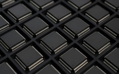
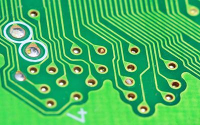
Semiconductors
Nordic Semiconductor is a fabless semiconductor company specializing in wireless technology that powers the IoT.
181 Posts

Intrinsic ID
Semiconductor
Securing the IoT with the World's Top PUF Technology. Authenticate Everythi...
16 Posts
View more
Latest Posts


New fabs will focus on making cutting-edge chips, not those based on older, established technology. So how should your company solve for potential limited supplies?

4 minutes read

ASIC design is the specialized practice of developing chips tailored to perform specific tasks with maximum efficiency, precision, and reliability—combining architectural insight, hardware expertise, and careful trade-offs to meet exact functional and system-level requirements.
Discover what tented vias are in PCB design and how to use them effectively – covering their definition, benefits, drawbacks, and best practices from design through manufacturing!

Review of industrial applications of printed electronics - what are current successful applications?
TechBlick's presentation reviews printed electronics' industrial applications, dispelling the notion that it's solely a technology of the future. The talk showcases various commercial success stories incl. photovoltaics, displays, sensors, HMIs, 3D electronics, MLCCs, PCBs, semicon packaging, etc


SystemVerilog is the industry's leading hardware description and verification language (HDVL), offering a unified solution for digital system design and verification. This article delves into the fundamentals of SystemVerilog, highlighting its origins, key differences from Verilog, essential language elements, design constructs, and powerful verification features.

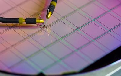
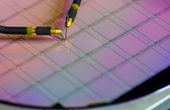
Wafer Probing is an electrical testing process conducted on semiconductor wafers after the integrated circuits are applied to the wafers. This is an essential step in the semiconductor manufacturing process that helps to determine the functionality of wafers and overall production quality. This article explores the process, importance, types, and applications of wafer probing.

Thin film deposition is a process used to create thin film coatings on different materials. Thin films can consist of metal, semiconductors, and dielectrics, providing them with different properties. These properties translate to benefits such as electrical insulation, optical transmission, and corrosion resistance, that can be used to improve substrate performance. This article explores the processes of thin film deposition, along with its types, parameters, benefits, drawbacks, and applications.

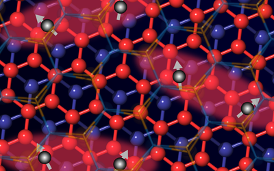
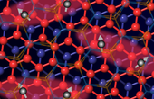
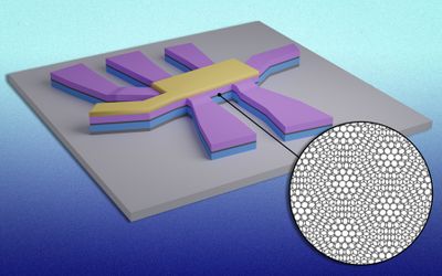
Nearly a decade ago, researchers heralded the discovery of a new wonder class of ultrathin materials with special optical and electrical properties that made it a potential rival for graphene, a form of carbon discovered in 2004 whose own special properties interest both scientists and engineers.

3 minutes read

EPFL researchers have come up with a new approach to electronics that involves engineering metastructures at the sub-wavelength scale. It could launch the next generation of ultra-fast devices for exchanging massive amounts of data, with applications in 6G communications and beyond.

3 minutes read


With more IoT devices performing mission-critical tasks - security is essential. To achieve the potential of smart devices that implement ML and AI in their applications, we must protect the critical intellectual property that represents the majority of the solution’s value.

A quick electric pulse completely flips the material’s electronic properties, opening a route to ultrafast, brain-inspired, superconducting electronics.

Trustworthy and reliable applications are fueling the worldwide IoT success story. This article explains why protecting IoT edge devices is crucial in an environment with threats on the rise.


Advancements in power storage devices, Micro Electro Mechanical Systems (MEMS), Gallium Nitride (GaN) semiconductors, etc. are key to achieving carbon neutrality in various industries.

4 minutes read


It is hard to think of a profession facing a more trying set of circumstances than farming. Climate change has brought higher temperatures and lower winter rainfall. Soil erosion, a loss of biodiversity, as well as myriad pests and diseases add to the farmer’s burden.

4 minutes read