Cutting-Edge Methods of Solder Paste Application for Electronics Manufacturing
Explore key methods like Direct Ink Writing, screen printing, and jet dispensing, and learn how Voltera’s V-One and NOVA are transforming the solder paste application process for improved accuracy and efficiency.

05 Sep, 2024. 8 minutes read
The solder paste application process on printed circuit boards (PCBs) and flexible circuits can be challenging, as even the slightest deviation can lead to issues such as poor conductivity and component misalignment. Precise solder paste dispensing is crucial for the general performance of the electrical circuits as it directly affects the electrical connection between the components and the conductive traces.
This article discusses various techniques used for solder paste dispensing, including Direct Ink Writing (DIW), screen printing, and jet dispensing, and how Voltera's V-One and NOVA, are revolutionizing the solder paste application process by making it more precise, efficient, and accessible.
Understanding Solder Paste and Its Importance
Composition and Function of Solder Paste
Solder paste is a complex material composed of metal alloy powder and flux. The metal alloy powder, typically made of a combination of metals such as tin, lead, or bismuth, provides the necessary metallic content to melt and form solder joints during the reflow soldering process. The flux, on the other hand, helps clean the metal surfaces by removing oxides, ensuring that the solder adheres properly to the components and electrical pads. It also protects the solder paste from oxidizing during heating, which could otherwise weaken the resulting joints.
During the reflow soldering process, the paste is heated until the metal alloy melts, which allows it to flow and fill the gaps between the component leads and electrical pads. As it cools and solidifies, it forms electrical and mechanical connections essential for the proper functioning of the electronic device.
Another important consideration regarding the composition of solder paste is whether to use leaded or unleaded varieties. Leaded solder pastes, typically composed of tin-lead alloys, have been widely used due to their low melting point and excellent joint reliability. Due to health and environmental concerns, unleaded solder pastes, often made of tin-bismuth alloys, have become increasingly significant. However, unleaded pastes usually require higher temperatures for reflow, which can affect the process and the choice of materials used in PCBs and components.
Challenges in Solder Paste Application
The main challenge in solder paste application is achieving consistent deposition, as variations in the amount of paste deposited can cause significant issues. On the one hand, insufficient solder can cause weak joints, poor electrical connections, or tombstoning. On the other hand, excessive solder can lead to bridging, where solder forms unintended connections between adjacent pads or leads, causing short circuits.
Similarly, even minor inconsistencies due to factors such as stencil design, paste viscosity, and printing technique can lead to significant defects during reflow soldering, particularly in achieving proper alignment between the solder paste and PCB pads. Misalignment can also result in poor electrical connections and weak joints, ultimately compromising the overall functionality of the PCB. Therefore, given the miniaturization of components and the growing complexity of modern PCBs, precise control over the paste amount and accurate alignment with PCB pads are essential to ensure reliable and fully functional circuits.
Solder Paste Dispensing Techniques
Direct Ink Writing (DIW)
Direct Ink Writing is an advanced precision dispensing technique that involves using a fine nozzle to dispense solder paste directly onto the PCB in a controlled manner. This method allows exceptional control over the amount and placement of solder paste, making it ideal for applications requiring high precision.
The DIW technique is particularly useful in scenarios where traditional methods like screen printing may fall short, such as in the production of complex or miniature PCBs. DIW helps to minimize waste, reduce the risk of defects, and ensure that each connection is made exactly as intended for its pinpoint accuracy. DIW can also be used on a variety of substrates, including flexible and stretchable materials, and it is highly suitable for prototyping, iterations, and small-volume production.
Screen Printing
Screen printing is a more traditional method that uses a stencil with patterned openings to transfer solder paste onto a PCB. The process is known for its high throughput, making it ideal for mass production where large volumes of PCBs need to be processed quickly and efficiently.
However, while screen printing is effective for high-volume manufacturing, it has some limitations, particularly regarding precision. For instance, compared to more advanced techniques like DIW and jet dispensing, screen printing offers less accuracy. Achieving higher precision with screen printing requires high-precision stencils, which are expensive and time-consuming to develop. These stencils also wear out over time, necessitating frequent replacements, further increasing costs.
Jet Dispensing
Jet dispensing is another advanced technique used in high-precision applications. Jet dispensing does not require a stencil. Instead, it uses a nozzle to jet droplets of solder paste onto the PCB at high speeds. The key advantage of jet dispensing is its flexibility, as it can apply solder paste to small areas that are difficult to reach with other techniques, such as densely packed or irregularly shaped components. The ability to control the size and placement of droplets makes jet dispensing ideal for applications where accuracy is critical.
However, this precision and flexibility come at a higher cost than other methods like DIW, as jet dispensing systems are more complex and expensive in terms of initial setup and ongoing maintenance. The equipment requires regular calibration to maintain accuracy, and the higher precision often leads to slower throughput, further increasing operational costs.
Voltera's Solutions for Solder Paste Dispensing
Voltera's V-One and NOVA platforms leverage the precision of advanced direct ink writing technology to offer specialized solutions for both rigid and flexible electronics.
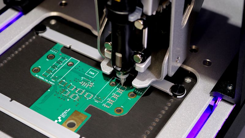
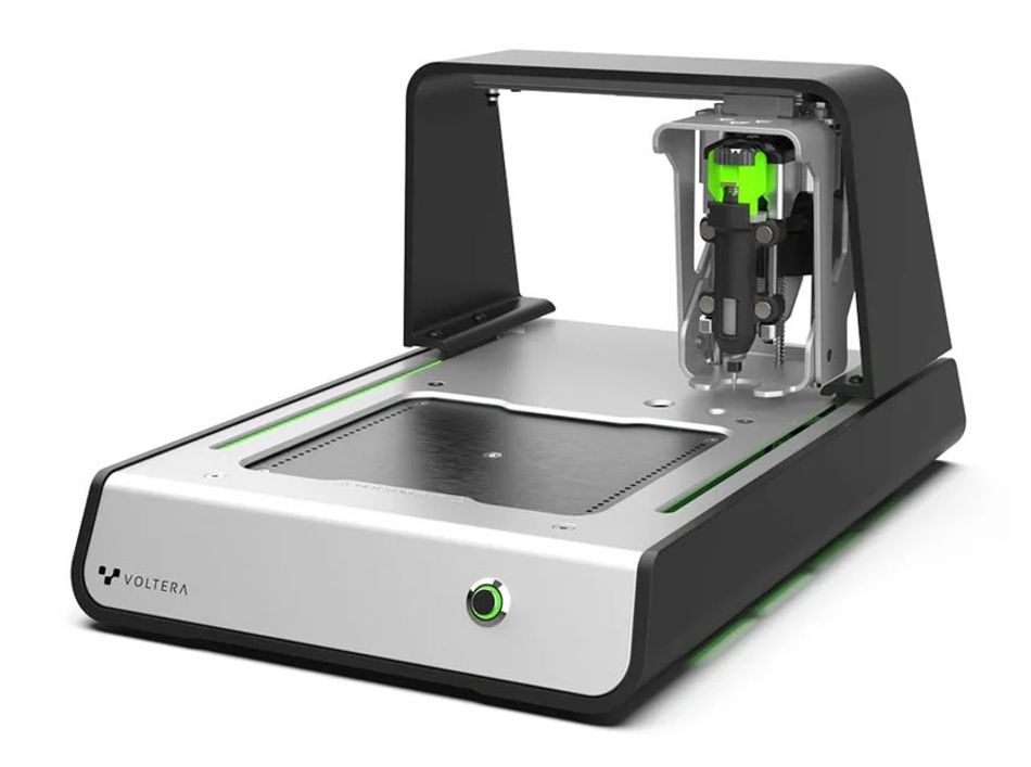
Voltera V-One for Rigid Electronics
The Voltera V-One is a desktop PCB printer designed for rigid electronics that use substrates like Flame Retardant 4 (FR4) and Flame Retardant 1 (FR1). It employs a direct ink writing process to dispense solder paste onto the PCB, allowing precise control over the amount and placement of solder paste, minimizing inconsistencies and bridging risks. The V-One's unique capabilities streamline the prototyping process by enabling solder paste to be dispensed directly after printing and curing conductive traces. It can also reflow the solder paste after components are placed, eliminating the need to transfer the board to a separate oven. This integrated workflow significantly reduces turnaround time and facilitates rapid iterations.
Similarly, the V-One's software allows users to select specific features for solder paste dispensing, enabling on-the-fly adjustments and rework. If a feature is unsatisfactory, it can be easily removed and re-dispensed by simply selecting it again in the software. This flexibility accelerates the design iteration process and empowers users to refine their prototypes with minimal effort.
Moreover, the V-One’s user-friendly interface simplifies operation and makes it accessible to users of all skill levels. The platform's efficiency and flexibility further enhance its appeal, allowing users to tailor the dispensing process to their specific needs.
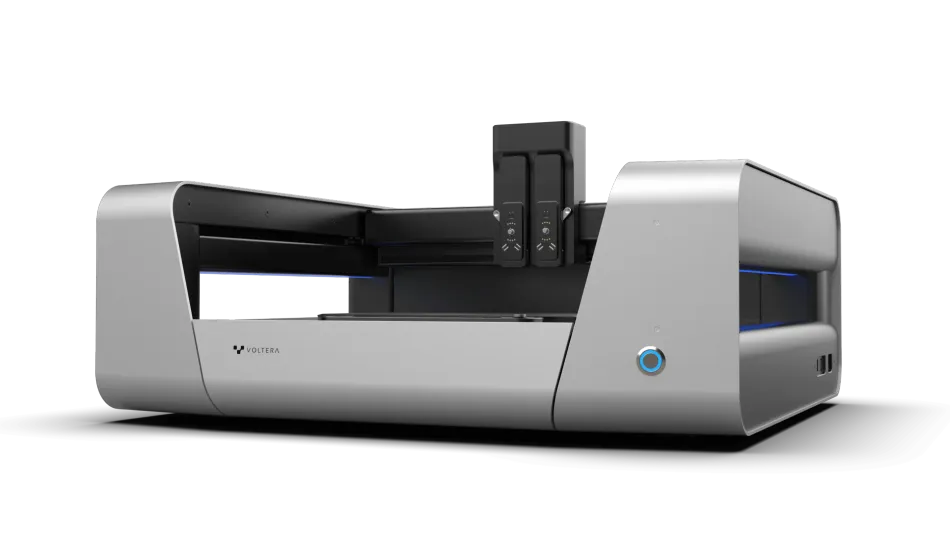
Voltera NOVA for Flexible, Stretchable Circuits
The Voltera NOVA is a specialized materials dispensing platform designed for printing electronics on flexible and stretchable substrates. It also utilizes a direct ink-writing process to dispense solder paste onto these unconventional materials. NOVA's precision in solder paste application is crucial for developing advanced flexible circuits, as it ensures accurate and consistent connections between components and the substrate.
NOVA's unique benefit lies in its ability to work with a wide range of substrates like polyimide, polyethylene terephthalate (PET), thermoplastic polyurethane (TPU), papers, and textiles. This versatility allows users to create innovative electronic devices that can conform to complex shapes and integrate seamlessly into various environments. Additionally, NOVA's high precision (0.1 mm trace width) and flexibility support cutting-edge applications in wearable technology and smart textiles. For instance, it can be used to create flexible biomedical sensors, electroluminescent displays for smart packaging applications, or to integrate electronics into wearables such as clothing and other textiles.
Practical Applications and Use Cases of Voltera's V-One and NOVA
Rigid PCB Prototyping with V-One
The V-One has found widespread application in the prototyping and small-scale production of rigid PCBs across various industries. The V-One has been used to quickly prototype and iterate on PCB designs for everything from solar shingles to IoT devices. Its ability to apply solder paste with precision ensures that each prototype functions correctly, allowing engineers to test and refine their designs before moving on to full-scale production. For example, at Princeton University, mechanical and aerospace engineering students are using Voltera's V-One PCB printer to design and build CubeSats, miniature satellites for space research.
The V-One enables hands-on learning, allowing students to gain a deeper understanding of electronic circuitry by being involved in every stage, from design to launch. The printer's user-friendly interface facilitates rapid prototyping, helping students see their projects through from concept to orbit. This practical experience enhances students’ comprehension of complex engineering processes, ensuring they are well-prepared for future innovations in space exploration.
Flexible Electronics with NOVA
Voltera's NOVA has been instrumental in developing flexible, stretchable circuits for various innovative applications. For instance, MIT researchers leveraged the Voltera NOVA system to print high-performance field electron emitters using a carbon nanotube (CNT) ink, demonstrating potential applications in space propulsion. The NOVA's direct-ink writing technology enabled the precise fabrication of these emitters, overcoming traditional semiconductor fabrication challenges. This innovative approach showcases the NOVA's capability to produce flexible, stretchable circuits for advanced applications like small satellite propulsion.
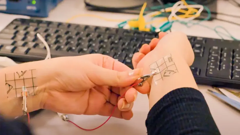
NOVA's ability to work with unconventional substrates makes it a useful tool in the automotive industry, where flexible electronics are increasingly used to create lightweight, adaptable components. Similarly, researchers from York University have used NOVA to develop electrodes printed on tattoo paper, offering a flexible, comfortable alternative to traditional electrodes used in ECG, EMG, and EEG procedures. In another application, Voltera demonstrated NOVA's precision by printing RFID tags with copper ink on paper, with the performance of the final tag exceeding that of off-the-shelf RFID tags from market leaders.
Leveraging Voltera's Resources for Success
Guides and Tutorials
Voltera guides and tutorials equip users with the knowledge and skills necessary to achieve optimal results. To support users in mastering solder paste dispensing with their V-One and NOVA platforms, Voltera offers a comprehensive library of detailed guides and tutorials. These resources provide users with information on how to overcome common challenges and optimize their solder paste dispensing processes.
For instance, their webinar “Dispensing Solder Paste on Factory Fabricated PCBs” provides a live demonstration of V-One, best practices for aligning your factory fabricated board and a sample of a completed curated print. Similarly, their support articles, like a step-by-step guide on the reflow process and purging solder paste, provide the users with step-by-step instructions and troubleshooting tips.
These resources represent just a glimpse of the extensive library Voltera offers. Whether you're a seasoned user or new to solder paste dispensing, Voltera's guides and tutorials empower you to confidently navigate the process and achieve high-quality results.
Conclusion
Precise solder paste dispensing is a critical factor in the success of electronics development since it ensures that PCBs are reliable, durable, and capable of performing as intended. Advanced techniques such as DIW, screen printing, and jet dispensing each offer unique advantages, allowing manufacturers to choose the best-suited method for their needs.
Voltera's V-One and NOVA represent cutting-edge solder paste application technology. The V-One excels in the prototyping of rigid electronics, offering precision and efficiency, while NOVA opens up new possibilities in flexible and stretchable circuits. By leveraging these tools and the accompanying resources, manufacturers can develop high-quality, reliable electronic devices with greater efficiency.
Discover How Voltera's Advanced Solder Paste Solutions Can Enhance Your Electronics Development
Visit Voltera's website to learn more about their cutting-edge solutions for solder paste dispensing. If you're ready to discuss how Voltera's advanced solder paste solutions can enhance your electronics development, you can book a meeting directly with the team:
References
Benedict O'Neill (2024) How Precision 3D Printing Enables Miniaturized Electric Space Propulsion [Online] Wevolver, Available at: https://www.wevolver.com/article/how-precision-3d-printing-enables-miniaturized-electric-space-propulsion (Accessed on August 22, 2024)
NOVA. The future of printed electronics [Online] Voltera, Available at: https://www.voltera.io/nova (Accessed on August 22, 2024)
Printed Tattoo Electrodes: Cutting-Edge Biomedical Monitoring. (2023) [Online] Voltera, Available at: https://www.voltera.io/blog/printed-tattoo-electrodes (Accessed on August 22, 2024)
Tech specs [Online] Voltera, Available at: https://www.voltera.io/tech-specs (Accessed on August 22, 2024)
Voltera [Online] Wevolver, Available at: https://www.wevolver.com/profile/voltera (Accessed on August 22, 2024)
V-One. PCB prototyping made easy [Online] Voltera, Available at: https://www.voltera.io/v-one (Accessed on August 22, 2024)
Printing an RFID Tag with Copper Ink on Paper [Online] Voltera, Available at: https://www.voltera.io/application-whitepapers/printing-rfid-tag-copper-ink-paper?utm_campaign=Wevolver&utm_source=Wevolver&utm_content=RFID%20white%20paper