How Does a Diode Work: Unraveling the Heart of Electronic Control
This article delves into the inner workings of a diode, exploring the principles that govern its ability to act as a one-way valve for current, as well as its varieties, characteristics, and vital significance in modern electronics.

09 Jul, 2024. 19 minutes read
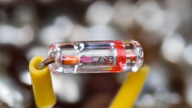
Old Germanium point-contact diode in sealed glass tube
Introduction
Diodes are fundamental components in modern electronics, serving as the building blocks for countless devices and circuits. But how does a diode work? This seemingly simple semiconductor device plays a crucial role in controlling the flow of electric current, allowing it to pass in one direction while blocking it in the reverse direction. This unique property makes diodes essential in applications ranging from power supplies and signal processing to digital logic and optoelectronics.
By understanding how a diode works, we gain a deeper appreciation for the foundation upon which complex electronic systems are built. This requires delving into concepts such as band theory, which explains how electrons behave in solid materials. Throughout this article, we will explore the internal mechanisms of a diode, uncovering the intricate relationship between voltage, current, and the magic of the p-n junction. How does a diode work? Still, curious about it? Let’s start with the foundational principles of semiconductors!
The Building Blocks: Diode Structure and Materials
Semiconductor Foundations
Semiconductors are materials with electrical conductivity between that of conductors and insulators. Silicon and germanium are the most common semiconductor materials used in diode fabrication. These elements have four valence electrons, forming covalent bonds with neighboring atoms in a crystal lattice structure.
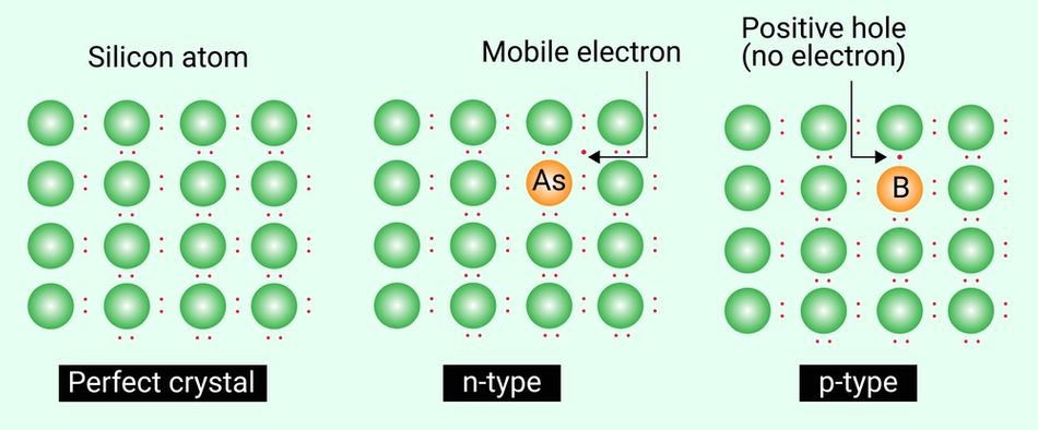
Doping is a crucial process in creating P-type and N-type semiconductors. By introducing impurities into the pure semiconductor, we can alter its electrical properties. N-type doping adds elements with five valence electrons (e.g., phosphorus), introducing extra electrons as charge carriers. P-type doping uses elements with three valence electrons (e.g., boron), creating "holes" or electron deficiencies as charge carriers. [1]
Band theory explains the behavior of electrons in semiconductors. It describes allowed energy states (bands) and forbidden energy states (band gaps). The valence band contains bound electrons, while the conduction band contains free electrons that contribute to electrical conductivity. The energy difference between these bands is the band gap, which determines the electrical properties of a material.
Carrier concentration refers to the number of charge carriers (electrons or holes) per unit volume in a semiconductor. Mobility describes how easily these carriers move through the material under an applied electric field. Both factors significantly influence the conductivity of semiconductors and are affected by doping levels and temperature.
The Fermi level is a crucial concept in semiconductor physics, representing the energy level with a 50% probability of being occupied by an electron at thermal equilibrium. In intrinsic semiconductors, the Fermi level lies near the middle of the band gap. Doping shifts the Fermi level, affecting the electrical properties of material and behavior in devices like diodes.
Several key properties of semiconductors play a crucial role in how diodes function. Here are these:
Bandgap Energy determines the energy required to excite an electron from the valence band to the conduction band, influencing conductivity.
Intrinsic Carrier Concentration defines the number of free electrons and holes within the material itself.
Electron and Hole Mobilities dictate how easily these charge carriers move under an applied electric field.
Dielectric Constant affects the electric field strength within the semiconductor.
Thermal Conductivity influences heat dissipation, important for high-power applications.
Recombination and generation rates determine how readily electrons and holes recombine or are generated, impacting current flow within the device.
Understanding these properties is essential for designing and optimizing diodes for specific functionalities.
Recommended Reading: What is a Semiconductor? A Comprehensive Guide to Engineering Principles and Applications
P-N Junction: The Core of a Diode
The P-N junction forms when P-type and N-type semiconductors are brought into contact. This junction is the fundamental building block of diodes and many other semiconductor devices. Upon contact, the concentration gradient causes electrons from the N-type region to diffuse into the P-type region, while holes from the P-type region diffuse into the N-type region.
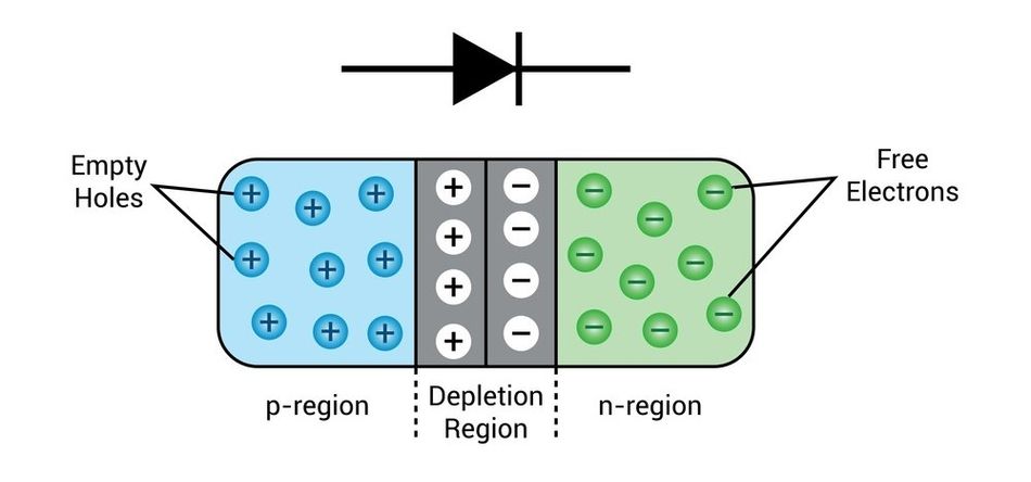
Once electrons and holes diffuse across the junction, they leave behind ionized donors and acceptors, respectively. This creates a region depleted of mobile charge carriers, known as the depletion region. The significance of this region lies in its high resistance and the presence of an internal electric field, which is crucial for diode operation.
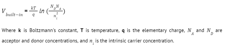
The diffusion of carriers across the junction creates a built-in potential (V) and an associated electric field. This potential barrier prevents further net diffusion of carriers once equilibrium is reached. The built-in potential can be expressed as:
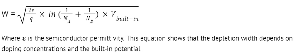
The width of the depletion region (W) can be derived using the depletion approximation and Poisson's equation. For an abrupt junction:
Two types of currents exist in the P-N junction: drift and diffusion. Drift current is caused by the electric field in the depletion region, which sweeps minority carriers across the junction. Diffusion current results from the concentration gradient of carriers across the junction. At equilibrium, these currents balance each other, resulting in zero net current flow.
The movement of electrons and holes at the junction is governed by complex quantum mechanical processes. Electrons in the conduction band of the N-type region can overcome the potential barrier and enter the P-type region, where they become minority carriers and quickly recombine with holes. Similarly, holes from the P-type region can enter the N-type region. This continuous process of carrier injection and recombination maintains the equilibrium carrier concentrations on both sides of the junction.
The behavior of carriers at the junction is described by the continuity equation, which relates the time rate of change of carrier concentration to the generation, recombination, and transport of carriers. This equation, combined with Poisson's equation and the current density equations, forms the foundation for understanding the detailed physics of P-N junctions and diode operation.
Recommended Reading: Understanding N-Type vs P-Type Semiconductors
Diode Physics: How the Magic Happens
Forward Bias Operation
Forward bias occurs when a positive voltage is applied to the P-type region relative to the N-type region of a diode. This applied voltage reduces the built-in potential barrier at the P-N junction, narrowing the depletion region and allowing for significant current flow. When a diode is forward-biased, current flows through the device from the anode to the cathode.
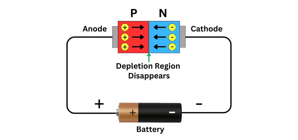
As the forward bias voltage increases, the potential barrier decreases, enabling more majority carriers to diffuse across the junction. Electrons from the N-type region flow into the P-type region, while holes from the P-type region flow into the N-type region. This results in a net current flow from the P-type to the N-type region.
The current-voltage relationship in a forward-biased diode is described by the Shockley diode equation:
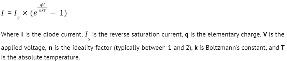
This equation accounts for both the diffusion and recombination currents in the diode.
Minority carrier injection is a crucial process in forward bias operation. As the barrier is lowered, electrons (minority carriers) are injected into the P-type region, and holes (minority carriers) are injected into the N-type region. These injected minority carriers recombine with majority carriers, maintaining charge neutrality. The recombination process occurs through various mechanisms, including radiative, Auger, and Shockley-Read-Hall recombination. [2]
Under forward bias, the concept of quasi-Fermi levels becomes important. The quasi-Fermi levels describe the separate electrochemical potentials for electrons and holes when the device is not in thermal equilibrium. The separation of quasi-Fermi levels determines the voltage across the device and influences the carrier concentrations and current flow.
The key points about forward bias behavior include:
Reduction of the built-in potential barrier
Narrowing of the depletion region
Exponential increase in current with applied voltage
Minority carrier injection across the junction
Recombination of injected carriers in neutral regions
Deviation from ideal behavior due to series resistance and high-level injection effects
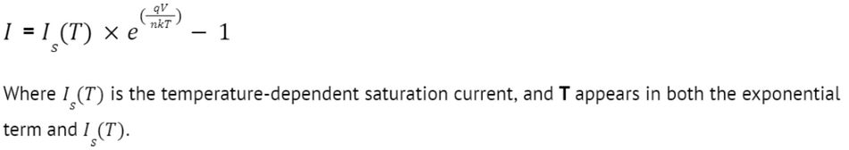
Temperature dependence of current due to the exponential term in the Shockley equation
The voltage drop across the diode is typically around 0.6 - 0.7 V for silicon diodes at room temperature
Reverse Bias Operation
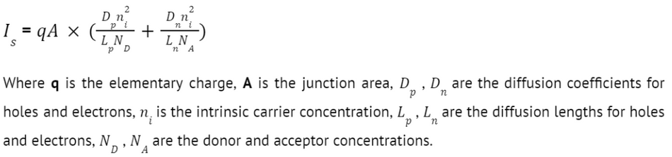
Reverse bias occurs when a negative voltage is applied to the P-type region relative to the N-type region of a diode. Under these conditions, the diode exhibits significantly different behavior compared to forward bias.
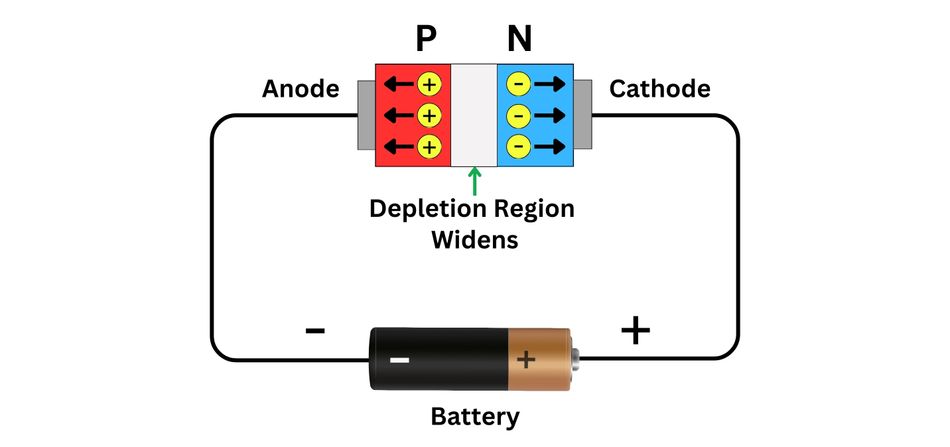
The applied reverse voltage increases the potential barrier at the P-N junction, causing the depletion region to widen. This widening occurs as more charge carriers are swept away from the junction, leaving behind additional ionized donors and acceptors. The expanded depletion region results in a high-resistance path, allowing only a small reverse saturation current (Is) to flow.
The reverse saturation current is primarily due to thermally generated electron-hole pairs in the depletion region and can be modeled mathematically as:
Once the reverse voltage increases, the diode maintains its high-resistance state until it reaches the reverse breakdown voltage. At this point, one of two breakdown mechanisms occurs:
Avalanche Breakdown: In lightly doped junctions, high electric fields accelerate carriers to energies sufficient to create electron-hole pairs through impact ionization. This process creates a cascade effect, leading to a sudden increase in current.
Zener Breakdown: In heavily doped junctions, the electric field becomes strong enough to pull electrons directly from the valence band to the conduction band through quantum tunneling. This occurs at lower voltages than avalanche breakdown.
Both breakdown mechanisms result in a sharp increase in current at the reverse breakdown voltage, which can be utilized in voltage regulator applications.
| Characteristic | Forward Bias | Reverse Bias |
| Applied Voltage | Positive to P, Negative to N | Negative to P, Positive to N |
| Depletion Region | Narrows | Widens |
| Current Flow | The exponential increase in voltage | Very small, nearly constant until a breakdown |
| Resistance | Low | High |
| Voltage Drop | ~0.6 - 0.7 V (Si) | Can be very high (up to breakdown voltage) |
| Carrier Behavior | Majority carrier injection | Minority carrier drift |
| Main Application | Conducting current | Blocking current, voltage regulation (in breakdown) |
| Temperature Effect | Current increases with temperature | Reverse current doubles approximately every 10°C |
Recommended Reading: Forward Bias, Reverse Bias and their effects on Diodes
Diode Varieties: Beyond the Basics
Zener Diodes: Voltage Regulation Masters
Zener diodes are specialized diodes designed to operate in the reverse breakdown region without damage. Their unique property is a highly stable reverse breakdown voltage, making them ideal for voltage regulation applications.
In voltage regulation, Zener diodes maintain a constant voltage across their terminals over a wide range of current conditions. They are commonly used in power supplies, voltage reference circuits, and overvoltage protection systems.
The Zener effect occurs in heavily doped p-n junctions when a strong electric field enables electrons to tunnel directly from the valence band to the conduction band. This happens at relatively low voltages (below about 5 volts). For higher voltages, avalanche breakdown dominates, where impact ionization creates a multiplication of charge carriers. Both mechanisms can coexist in Zener diodes.
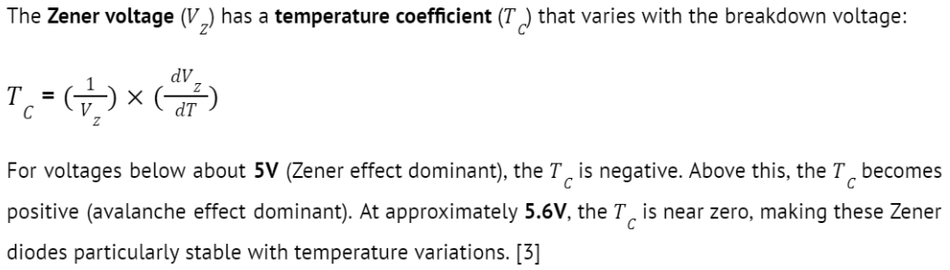
The temperature dependence impacts the voltage regulation performance. Positive TC Zener diodes tend to have better voltage regulation but higher noise, while negative TC types have lower noise but poorer regulation.
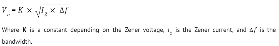
Zener diodes exhibit two main types of noise:
Burst (popcorn) Noise: Random, sudden changes in current, more prominent in lower voltage Zeners.
Avalanche Noise: White noise caused by the random nature of the avalanche process, more significant in higher voltage Zeners.
The noise voltage can be approximated by:
Understanding these characteristics allows engineers to select the appropriate Zener diode for specific applications, balancing voltage stability, temperature performance, and noise requirements.
Light-Emitting Diodes (LEDs): Illuminating the World
Light-Emitting Diodes (LEDs) are semiconductor devices that convert electrical energy directly into light through the process of electroluminescence. The operating principle of LEDs is based on radiative recombination of electron-hole pairs in a forward-biased p-n junction.
When a forward bias is applied, electrons from the n-type region and holes from the p-type region are injected into the active region. In this region, electrons in the conduction band recombine with holes in the valence band, releasing energy in the form of photons. This process is called radiative recombination.
The color of light emitted by an LED is determined by the bandgap energy of the semiconductor material used. The relationship between the bandgap energy (Eg) and the wavelength of emitted light (λ) is given by:

Where h is Planck's constant and c is the speed of light.
Different types of LEDs produce various colors:
Gallium Arsenide (GaAs): Infrared
Gallium Arsenide Phosphide (GaAsP): Red to orange
Aluminum Gallium Indium Phosphide (AlGaInP): Red to yellow
Gallium Nitride (GaN): Blue
Indium Gallium Nitride (InGaN): Blue to green
White LEDs are typically created using blue LEDs with a yellow phosphor coating or by combining red, green, and blue LEDs.
The efficiency of LEDs is characterized by two main factors:
Internal Quantum Efficiency (IQE): The ratio of photons generated to electrons injected.
Light Extraction Efficiency (LEE): The fraction of generated photons that escape the device.
The overall efficiency, or External Quantum Efficiency (EQE), is the product of IQE and LEE. Modern LEDs can achieve EQE values exceeding 50% for some colors.
Advancements in LED technology focus on improving efficiency, color rendering, and reducing costs, making LEDs increasingly prevalent in lighting, displays, and communication applications.
Schottky Diodes: Speed Demons of the Diode World
Schottky diodes, also known as hot carrier diodes, are unique semiconductor devices that use a metal-semiconductor junction instead of a p-n junction. This structure gives Schottky diodes distinct properties that make them ideal for high-speed switching applications.
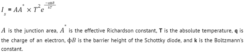
The key feature of a Schottky diode is the Schottky barrier, formed at the interface between a metal and an n-type material. This barrier is characterized by its height (φB), which is the potential difference between the metal work function and the semiconductor electron affinity.
The Schottky barrier height significantly impacts the diode's characteristics:
Forward Voltage Drop: Typically 0.2 - 0.3V, lower than conventional p-n junction diodes
Reverse Leakage Current: Generally higher due to thermionic emission over the barrier
Switching Speed: Extremely fast due to majority carrier conduction
The current-voltage relationship in a Schottky diode is described by:

Where I(s) is the saturation current, dependent on the barrier height:
Schottky diodes excel in high-speed switching applications due to their majority carrier conduction mechanism. Unlike p-n junction diodes, there's no minority carrier storage, eliminating reverse recovery time. This makes Schottky diodes ideal for applications including high-frequency rectifiers, clamping diodes in switching power supplies, RF mixers and detectors.
Hot carrier effects are prominent in Schottky diodes. When electrons gain enough energy to overcome the Schottky barrier, they can enter the metal with excess kinetic energy. This can lead to increased noise in the device and potential reliability issues due to hot carrier injection into the semiconductor. To mitigate these effects, modern Schottky diodes often incorporate guard ring structures and optimized doping profiles.
The unique properties of Schottky diodes make them indispensable in applications requiring ultra-fast switching and low forward voltage drop, despite their higher reverse leakage current and lower breakdown voltage compared to p-n junction diodes.
Tunnel Diodes: Quantum Mechanical Marvels
Tunnel diodes, also known as Esaki diodes, operate on the principle of quantum tunneling, a phenomenon where electrons can penetrate through potential barriers that they classically shouldn't be able to overcome. This unique behavior arises in heavily doped p-n junctions, where the depletion region is extremely narrow (typically less than 10 nm). [4]
The key feature of tunnel diodes is their negative differential resistance (NDR) region. As the forward bias increases from zero, the current initially increases due to increased tunneling. However, at a certain point, further increase in voltage leads to a decrease in current, creating the NDR region. This occurs because the number of electrons available for tunneling decreases as the conduction band of the n-region moves above the valence band of the p-region.
The energy band diagram of a tunnel diode changes significantly under different bias conditions:
Zero Bias: The Fermi levels in the p and n regions align, with a narrow depletion region between them.
Small Forward Bias: Electrons from the n-region can tunnel directly into empty states in the p-region, causing the flow of current.
Peak Current: The conduction band edge of the n-region aligns with the valence band edge of the p-region, maximizing the tunneling current.
Valley Current: Further increase in bias misaligns the bands, reducing tunnelling current to a minimum.
High Forward Bias: The diode behaves like a conventional p-n junction diode, with diffusion current dominating.
The NDR characteristic makes tunnel diodes valuable in high-frequency applications:
Oscillators: The NDR region allows for the creation of simple, compact oscillators that can operate at very high frequencies (up to hundreds of GHz).
Amplifiers: Tunnel diodes can be used as reflection amplifiers in microwave circuits, providing gain with minimal noise.
Switching Circuits: The rapid transition between peak and valley currents enables fast switching operations.
Tunnel diodes exemplify the practical application of quantum mechanics in electronic devices, enabling unique functionalities that are not possible with conventional semiconductor devices. Their ability to operate at extremely high frequencies makes them valuable in specialized RF and microwave applications, despite their limited use in general-purpose circuits. This is due to their specialized nature and manufacturing challenges.
Understanding these types of diodes and their unique characteristics empowers engineers to design efficient and effective electronic circuits. From signal processing to power management and light control, diodes play a vital role in shaping the technological landscape.
Recommended Reading: Zener Diode: A Comprehensive Guide to Its Principles and Applications
Diode Characteristics: Understanding the Numbers
I-V Characteristics: The Diode's Signature
The current-voltage (I-V) characteristic curve is a fundamental representation of a diode's electrical behavior. This curve illustrates the relationship between the current flowing through the diode and the voltage applied across it, providing crucial insights into the device's performance.
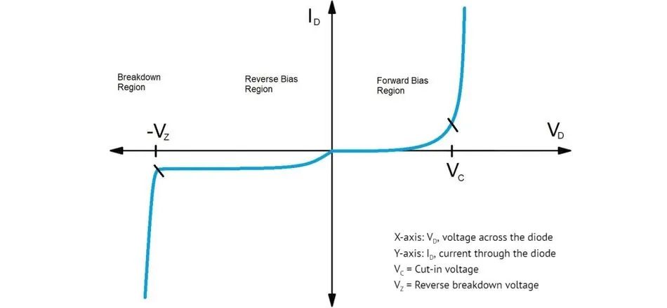
Key points on the I-V curve include:
Forward Bias Region: As positive voltage is applied, current increases exponentially.
Knee Voltage (Vk): The voltage at which current begins to increase rapidly (typically 0.6-0.7 V for silicon diodes).
Reverse Bias Region: Minimal current will flow once negative voltage is applied.
Reverse Breakdown Voltage (VBR): The point at which reverse current increases dramatically.
The ideal diode equation, also known as the Shockley diode equation, describes the I-V relationship:
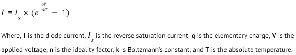
The ideal diode equation has limitations. It neglects the impact of series resistance within the diode, which can affect the actual voltage across the device. Additionally, it doesn't model the complex breakdown mechanism itself. Finally, the equation assumes low current levels, making it less accurate for high-power applications.
The ideality factor (n) is a measure of how closely the diode follows ideal behavior. Its physical significance lies in the dominant current transport mechanism:
n ≈ 1: Diffusion current dominates (ideal behavior)
n ≈ 2: Recombination current in the depletion region dominates
1 < n < 2: Both mechanisms contribute significantly
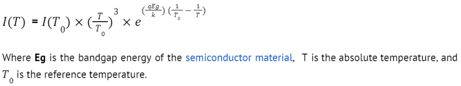
Temperature significantly affects the I-V characteristics:
Reverse saturation current (Is) doubles approximately every 10°C increase.
Forward voltage drop decreases by about 2mV/°C.
The entire I-V curve shifts with temperature changes.
The temperature dependence can be expressed as:
Understanding these characteristics is crucial for designing and analyzing diode-based circuits, as they directly impact the device's performance in various applications.
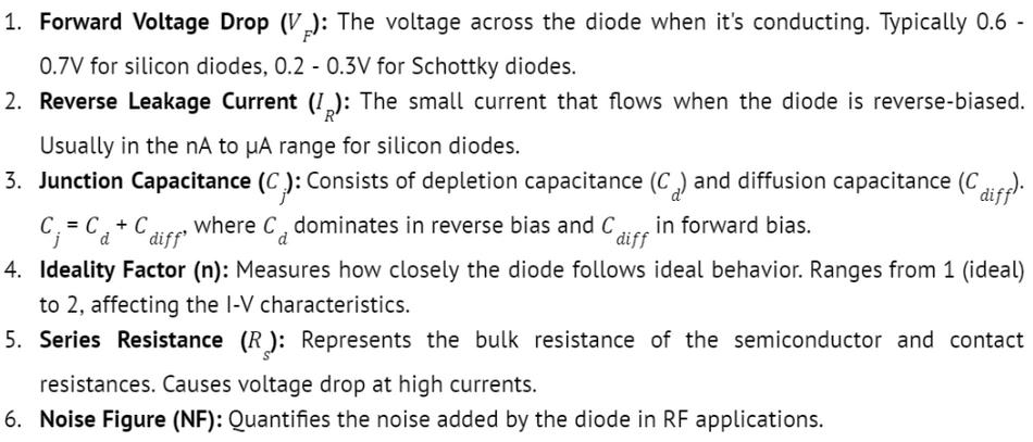
Key Diode Parameters
Diode performance is characterized by several key parameters that influence their behavior in electronic circuits:
Small Signal Model is ideal for analyzing AC behavior with small AC signals superimposed on a DC bias point. It typically represents the diode with a linear resistance, reflecting the change in current with respect to voltage around the operating point. This approach proves valuable in RF circuits, and small-signal amplifiers where the signal variations are small.
Large Signal Model is used for analyzing diode behavior with large signal swings. It is typically represented by a voltage-dependent current source in parallel with junction capacitance. Used in power electronics, rectifiers, and circuits with significant signal swings to analyze the non-linear behavior of the diode.
Several key diode parameters significantly impact their performance in circuits.
Forward Voltage Drop directly affects efficiency in power rectification applications, as a higher drop translates to wasted power.
Reverse Leakage Current, though ideally minimal, contributes to power consumption even in reverse bias.
Junction Capacitance limits switching speed in digital circuits, as it takes time to charge and discharge.
The Ideality Factor, a measure of non-ideality in current flow, influences the accuracy of logarithmic amplifiers.
Series Resistance, present within the diode itself, causes power loss and voltage drop, especially in high-current applications.
Finally, for radio frequency (RF) mixer and detector circuits, noise figure becomes a critical parameter, as it determines the amount of noise introduced by the diode itself. Understanding these parameters is crucial for optimizing diode selection and achieving desired circuit performance.
Understanding these parameters is crucial for selecting the appropriate diode for specific applications and predicting circuit behavior accurately.
Diodes in Action: Practical Applications
Diode is a fundamental semiconductor device that not only serves as a basic circuit element but also provides the template for the development of many critical electronic devices like transistors, power diodes, LEDs, etc. Let's explore some of their most practical applications:
Rectification: Converting AC to DC
Diodes allow current to flow in one direction while blocking it in the opposite direction. This directional property is known as rectification. Rectification is the process of converting alternating current (AC) to direct current (DC) using diodes. This fundamental application of diodes is crucial in power supplies and various electronic systems.
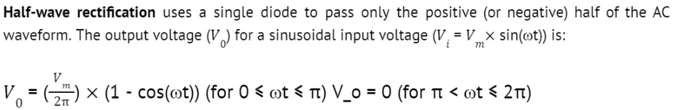
Full-wave rectification uses four diodes in a bridge configuration as diode bridge rectifier to utilize both halves of the AC waveform. The output voltage is:

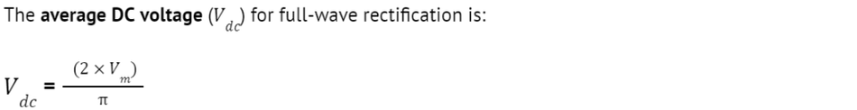
Ripple factor (r) quantifies the AC component remaining in the rectified output:

For half-wave rectification, r = 1.21, while for full-wave rectification: r = 0.48
Despite their function, diodes aren't perfect rectifiers. Here are the considerations:
Forward voltage drop lowers the output voltage, reducing efficiency.
Reverse leakage current creates unwanted power loss.
Junction capacitance causes current spikes during switching, hindering high-frequency operation.
These non-idealities necessitate careful selection and consideration when designing rectifier circuits.
Signal Clamping and Clipping
Diodes are extensively used in clamping and clipping circuits to modify signal waveforms.
Clamping shifts a signal's DC level without altering its shape. A basic clamper consists of a diode, capacitor, and resistor. The diode conducts during one part of the cycle, charging the capacitor, which then maintains the shifted DC level.
Clipping limits a signal's amplitude by removing portions that exceed a certain threshold. A simple clipper uses a diode in parallel with the load, conducting when the input exceeds the diode's forward voltage.
The transfer characteristic of an ideal clamping circuit is:

For a clipping circuit:

Diodes are versatile tools for manipulating signals. Clamping circuits excel at DC restoration in AC coupling, stabilizing baselines in communication systems, and safeguarding circuits from voltage spikes. Clipping, on the other hand, shapes waveforms for signal processing, regulates voltage in basic power supplies, reduces noise in digital circuits, and shields delicate electronic components from voltage surges.
These applications demonstrate the versatility of diodes in signal conditioning and circuit protection.
Voltage Protection: Guarding Against Overvoltage
Diodes play a crucial role in protecting electronic circuits from overvoltage conditions, which can damage sensitive components. Transient voltage suppression (TVS) diodes are specifically designed for this purpose, utilizing the avalanche breakdown phenomenon to clamp voltage spikes.
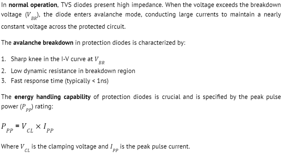
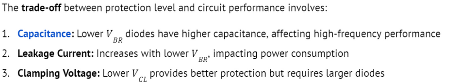
Selecting the optimal TVS diode requires balancing these factors against the specific circuit requirements and potential transient threats.
Advanced Applications: Pushing the Limits
Diodes enable various advanced applications that leverage their unique properties:
1. Voltage Multiplier Circuits: Diodes and capacitors can be arranged to produce output voltages higher than the input. The Cockcroft-Walton multiplier is a classic example:

2. Logarithmic Amplifiers: Exploiting the exponential I-V characteristic of diodes, log amps produce an output voltage proportional to the logarithm of the input:

Where n is the ideality factor, k is Boltzmann's constant, T is temperature, and q is electron charge.
3. Diode-based Temperature Sensors: The temperature dependence of the forward voltage drop is used for sensing:

Differential measurements with controlled current sources enhance accuracy.
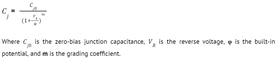
4. Varactor Diodes in Voltage-Controlled Oscillators (VCOs): The voltage-dependent capacitance of reverse-biased diodes tunes the oscillator frequency:
5. Diode Modeling for Circuit Simulation: Accurate diode models are crucial for circuit simulation. The SPICE diode model includes DC power characteristics, capacitance effects, temperature effects, and reverse breakdown.
6. More advanced models like VBIC or MEXTRAM provide higher accuracy for specialized diodes and extreme operating conditions.
These advanced applications demonstrate the versatility of diodes beyond basic rectification and switching, enabling complex analog and RF circuit designs.
Recommended Reading: Rectifier Diode: Revolutionizing Electrical Applications with Advanced Semiconductor Technology
Challenges and Considerations in Diode Technology
Temperature Effects on Diode Performance
Temperature significantly influences diode behavior, affecting various parameters:
Reverse saturation current (Is) doubles approximately every 10°C
Forward voltage (Vf) decreases by about 2mV/°C for silicon diodes
Breakdown voltage increases with temperature for avalanche breakdown, decreases for Zener breakdown.
The temperature dependence of the Shockley diode equation is expressed as:
Thermal runaway in power diodes occurs when increased current leads to higher temperature, further increasing current in a positive feedback loop. This can be mitigated by proper thermal management and current limiting.
Key considerations for temperature-sensitive applications include:
Accurate temperature modeling in circuit simulations
Thermal resistance and heat sinking for power diodes
Temperature coefficients of key parameters
Operating temperature range and derating factors
Stability of temperature compensation techniques over time and environmental conditions
High-Frequency Limitations
Diodes face several limitations in high-frequency applications:
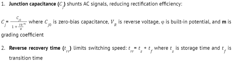
The small-signal equivalent circuit of a diode at high frequencies includes series resistance (rs), junction capacitance (Cj), diffusion capacitance (Cd) in forward bias and package inductance (Lp) and capacitance (Cp).
Package parasitics significantly impact high-frequency performance:
Lead inductance causes series resonance with junction capacitance
Package capacitance creates parallel resonance
Skin effect increases effective series resistance at high frequencies
Critical applications affected by these limitations include:
High-speed switching in digital circuits
RF mixers and detectors in communication systems
Fast-recovery rectifiers in switch-mode power supplies
Sampling circuits in high-speed data acquisition systems
Reliability and Radiation Effects
Diode reliability is crucial in many applications, with several failure mechanisms:
Electromigration: Ion transport in metallization under high current densities
Hot Carrier Injection: Energetic carriers trapped in oxide layers, altering device characteristics
Thermal Cycling: Mechanical stress due to thermal expansion mismatches
Contamination: Impurities introduced during manufacturing affecting device performance
Ionizing radiation effects on diodes include:
Increased reverse leakage current due to the generation of electron-hole pairs
Shift in forward voltage characteristics
Changes in breakdown voltage
Degradation of minority carrier lifetime
Radiation-hardening techniques for diodes:
Using wide bandgap materials (e.g., SiC, GaN)
Implementing guard rings to reduce surface leakage
Optimizing doping profiles for radiation tolerance
Employing epitaxial layers to minimize substrate effects
Single-event effects (SEE) in diodes:
Single-event transients (SET): Temporary voltage spikes due to particle strikes
Single-event burnout (SEB): Catastrophic failure in power diodes due to high-energy particles
SEE mitigation strategies include the use of redundant diodes in parallel, implementing current-limiting structures and employing fast-recovery diodes to minimize vulnerability window. Understanding these challenges and considerations is essential for designing robust and reliable diode-based circuits across various applications and environments.
Recommended Reading: Understanding Circuit Board Components: A Comprehensive Guide
Conclusion
Diodes bridge the gap between quantum mechanics and our everyday electronics. These versatile devices, from simple to complex, govern current flow through ingenious material properties. As we strive for ever-better performance, research delves into new materials, nanoscale structures, and architectures. This exploration promises to unlock the future of electronics in terahertz applications, quantum computing, and energy harvesting.
Frequently Asked Questions
Q. How does the reverse recovery time of a diode affect its high-frequency performance?
A. Reverse recovery time limits a diode's switching speed, impacting its high-frequency performance by introducing switching losses, generating noise and distortion, limiting the maximum usable frequency in rectification and switching applications
Q. What are the advantages of wide bandgap semiconductors in diode applications?
A. Wide bandgap semiconductors (e.g., SiC, GaN) offer several benefits including higher breakdown voltages, lower on-resistance, better thermal conductivity, improved radiation hardness and higher operating temperatures.
Q. How can the noise characteristics of Zener diodes be minimized in voltage reference applications?
A. To minimize Zener diode noise in voltage references, operate the diode at optimal current for minimum noise. You can use buried Zener structures to reduce surface noise, or implement noise filtering techniques. Users also consider compensation in temperature to stabilize noise performance.
Q. What techniques are used to enhance the radiation hardness of diodes for space applications?
A. Radiation hardening techniques for diodes include using epitaxial layers to minimize substrate effects, implementing guard rings to reduce surface leakage, optimizing doping profiles for radiation tolerance, employing redundancy and error correction in circuit design
Q. What are the key considerations when designing high-power diode circuits?
A. Key considerations for high-power diode circuits include thermal management and heat sinking, surge current and avalanche energy ratings, reverse recovery characteristics, voltage derating for reliability, and paralleling techniques for current sharing
References
[1] ScienceDirect. Implementing different dopants on Schottky Diodes [Cited 2024 July 05] Available at: Link
[2] Cadence. The Types of Recombination in Semiconductors [Cited 2024 July 05] Available at: Link
[3] Geeksforgeeks. Difference Between Zener Breakdown and Avalanche Breakdown [Cited 2024 July 05] Available at: Link
[4] Etechsparks. All About Tunnel Diode- Working Principle, Construction [Cited 2024 July 05] Available at: Link
Table of Contents
IntroductionThe Building Blocks: Diode Structure and MaterialsSemiconductor FoundationsP-N Junction: The Core of a DiodeDiode Physics: How the Magic HappensForward Bias OperationReverse Bias OperationDiode Varieties: Beyond the BasicsZener Diodes: Voltage Regulation MastersLight-Emitting Diodes (LEDs): Illuminating the WorldSchottky Diodes: Speed Demons of the Diode WorldTunnel Diodes: Quantum Mechanical MarvelsDiode Characteristics: Understanding the NumbersI-V Characteristics: The Diode's SignatureKey Diode ParametersDiodes in Action: Practical ApplicationsRectification: Converting AC to DCSignal Clamping and ClippingVoltage Protection: Guarding Against OvervoltageAdvanced Applications: Pushing the LimitsChallenges and Considerations in Diode TechnologyTemperature Effects on Diode PerformanceHigh-Frequency LimitationsReliability and Radiation EffectsConclusionFrequently Asked QuestionsReferences