How to Read a Circuit Board: Mastering the Language of Electronics
This article will guide you through the fundamentals of how to read a circuit board, decoding key elements, essential symbols and markings, exploring techniques for tracing circuits, and examining advanced analysis methods.

21 Oct, 2024. 21 min read
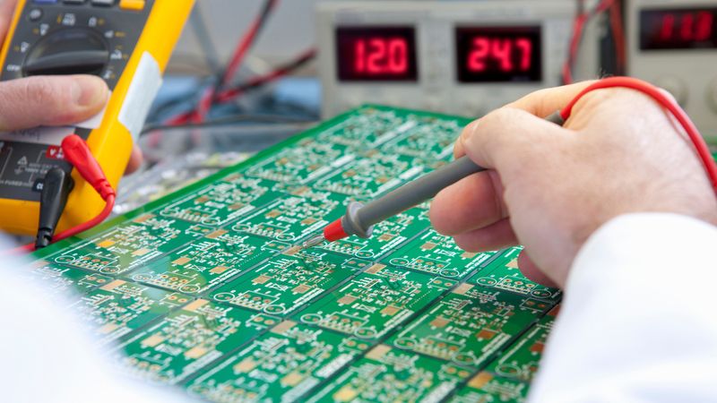
Circuit board being checked by an engineer using a test head connected to the Multimeter
Introduction
In electronics, circuit boards serve as the neural networks of devices, their components interconnected to perform specific functions. These intricate assemblies of components and conductive pathways are the backbone of everything from smartphones to industrial machinery. Understanding how to read a circuit board is an essential skill for anyone working with electronics. This enables efficient troubleshooting, design optimization, and innovation in electronic systems.
This article will guide you through the fundamentals of how to read a circuit board, decoding essential symbols and markings, exploring techniques for tracing circuits, and examining advanced analysis methods. By learning to decipher the symbols, markings, and layouts, you'll gain the ability to analyze circuit diagrams, troubleshoot malfunctions, and even design your own electronic projects. Still, curious about, how to read a circuit board? Let’s understand the macros, and their significance in Printed Circuit Board (PCB).
The Macros of Printed Circuit Board
Layers and Substrates
A printed circuit board (PCB) is a complex sandwich of materials, each layer serving a specific purpose in the overall functionality of the board. At its core, a PCB consists of alternating layers of conductive and insulating materials.
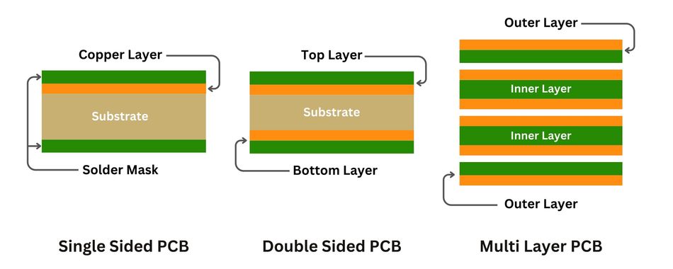
The foundation of a PCB is the substrate, typically made from FR-4 (Flame Retardant 4), a composite material of woven fibreglass cloth impregnated with an epoxy resin. [1] FR-4 is a material known for its excellent electrical insulation properties, mechanical strength, and resistance to moisture and chemicals. Other substrate materials include polyimide for high-temperature applications and ceramic substrates for specialized high-frequency circuits.
Copper layers are the conductive pathways of a PCB. In a simple two-layer board, copper foils are bonded to both sides of the substrate. Multi-layer boards stack additional copper and substrate layers, allowing for more complex circuit designs. These copper layers carry electrical signals and power throughout the board.

The solder mask is a thin layer applied over the copper layers, usually green in color. It serves to insulate the copper traces from accidental contact with other metal parts. This prevents solder bridges from forming between closely spaced solder pads and protects the copper from oxidation.
The outermost layer is the silkscreen, typically white in color. This layer contains text and symbols that provide valuable information for assembly, testing, and repair. Component designators, polarity indicators, and other identifying marks are printed on this layer.
In high-performance PCBs, additional specialized layers may be present. These can include embedded capacitance layers for improved power delivery, or dedicated ground planes for better signal integrity and electromagnetic interference (EMI) shielding.
Recommended Reading: PCB Layers: Everything You Need to Know
Essential Components
Circuit boards are populated with a variety of electronic components, each serving a specific function in the overall circuit design. Understanding these components is crucial for effectively reading and interpreting circuit boards.
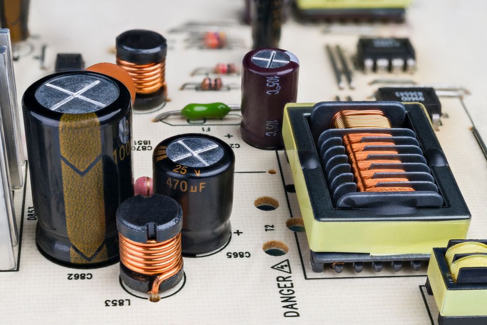
Resistors are passive components that resist the flow of electric current. They are typically small cylindrical or rectangular components with color-coded bands indicating their resistance value. Resistors are used for current limiting, voltage division, and biasing other components. When a variable resistor is used as a potential divider by using 3 terminals, it is called a potentiometer.
Capacitors store and release electrical energy. They come in various shapes and sizes, from small ceramic disc capacitors to larger electrolytic capacitors. [2] Capacitors are used for filtering, coupling, and decoupling in circuits.
Inductors store energy in a magnetic field when current flows through them. They are often coil-shaped and used in filters, oscillators, and power supplies. Inductors can also be used to smooth out voltage fluctuations and to create resonant circuits.
Diodes allow current to flow in only one direction. The most common types are rectifier diodes and light-emitting diodes (LEDs). They are used for rectification, signal detection, and visual indicators. Diodes can also be used as voltage regulators, switches, and clippers in electronic circuits.
Transistors are semiconductor devices that can amplify or switch electronic signals. Common types include bipolar junction transistors (BJTs) and field-effect transistors (FETs). BJTs are further divided into NPN and PNP transistors. They are fundamental to most electronic circuits, used in amplifiers, switches, and logic gates.
Integrated Circuits (ICs) are complex components that contain entire circuits within a single package. They can range from simple operational amplifiers to complex microprocessors. ICs are the building blocks of modern electronics, performing a wide range of functions.
Here's the table outlining the function of each component:
| Component | Function |
| Resistor | Limits Current Flow, Divides Voltage |
| Capacitor | Stores and Releases Electrical Energy |
| Inductor | Stores Energy in a Magnetic Field |
| Diode | Allows Current Flow in One Direction |
| Transistor (BJT) | Amplifies or Switches Electronic Signals |
| Integrated Circuit | Performs Complex Electronic Functions |
Understanding these essential components is crucial for interpreting circuit diagrams and analyzing the functionality of PCBs. In the following sections, we will explore how to read these components and interpret their markings.
Recommended Reading: Understanding Circuit Board Components: A Comprehensive Guide
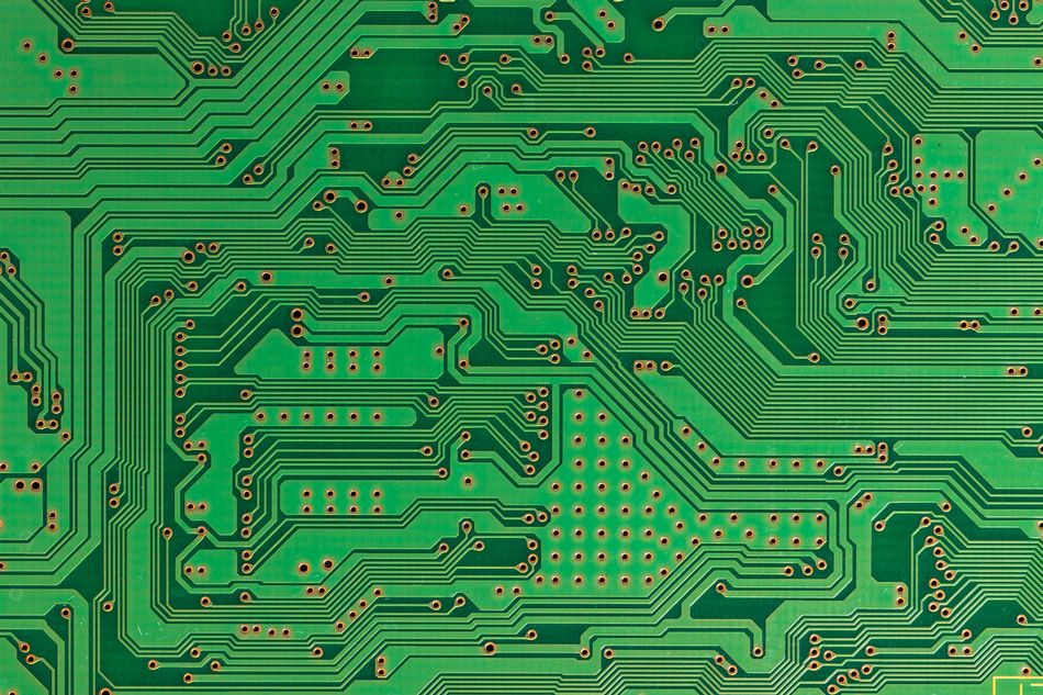
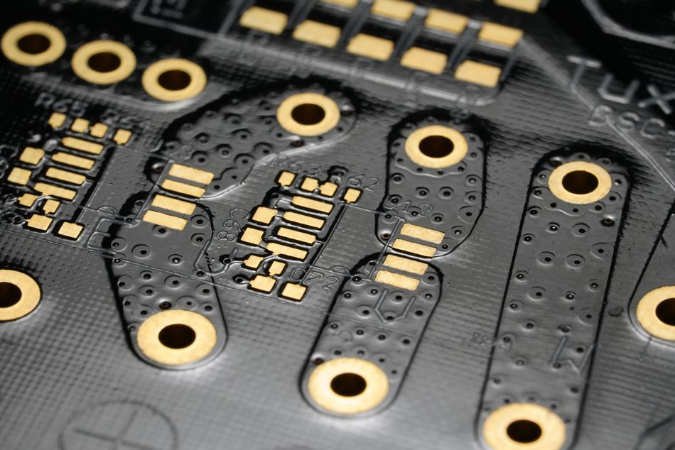
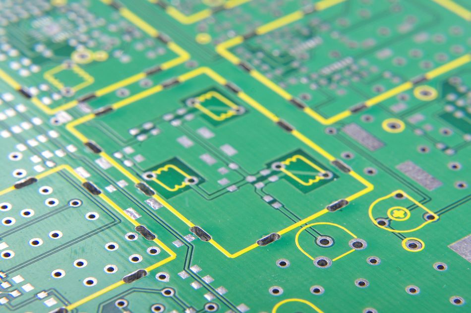
Traces and Vias
Traces are the lifeblood of printed circuit boards (PCBs), serving as the conductive pathways that connect various components and enable the flow of electrical signals. These thin copper lines are etched onto the board's surface and play a crucial role in determining the functionality and performance of PCBs.
There are three main types of traces in a PCB:
Signal Traces: These carry data signals between components, facilitating communication within the circuit. Signal traces require careful routing to maintain signal integrity and minimize interference.
Power Traces: Designed to deliver power from the supply to various components, power traces are typically wider than signal traces. This increased width helps accommodate higher current loads, reducing voltage drop and heat generation across the board.
Ground Traces: These connect all ground points in the circuit, establishing a common reference potential. Ground traces are essential for reducing noise and improving overall circuit performance.
In multi-layer PCBs, vias play a critical role in connecting traces between different layers. Via is a small hole filled with conductive material that allows electrical signals to pass from one layer to another. This enables the design of more complex circuits by efficiently routing connections across multiple layers without consuming additional board space.
There are three main types of vias used in PCBs:
Through-Hole Vias: These pass through the entire PCB, connecting the outer layers to the inner layers. They are the most common type and are used for connecting components or traces on both sides of the board.
Blind Vias: These connect an outer layer of the PCB to one or more inner layers but do not extend through the entire board. Blind vias are used to save space and improve routing density.
Buried Vias: These connect only the inner layers of a PCB, with no connection to the outer layers. Buried vias are typically used in high-density circuit designs to maximize available space and minimize signal interference.
Understanding the purpose and types of traces and vias is crucial for effectively reading and interpreting circuit board layouts, as well as for troubleshooting and designing PCBs.
Recommended Reading: PCB Trace: The Backbone of Modern Circuit Design
Decoding Circuit Board Symbols
Component Markings and Values
Understanding component markings and values is crucial for accurately reading and interpreting circuit boards. These markings provide essential information about each component's specifications and function within the circuit.
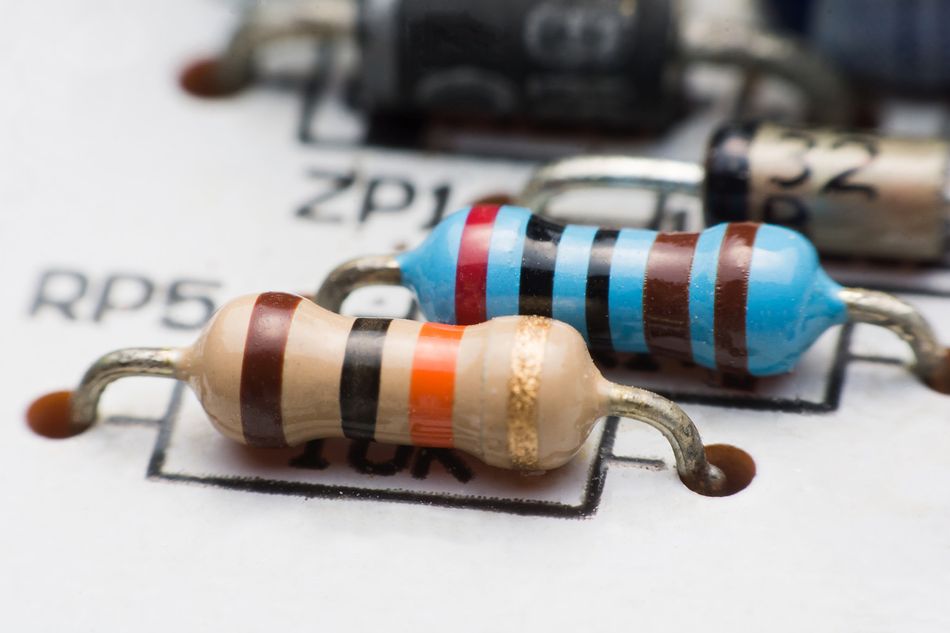
Resistors typically use color bands to indicate their resistance value and tolerance. The first two or three bands represent significant digits, the next band is the multiplier, and the final band indicates tolerance. For example, a resistor with bands colored brown, black, orange, and gold would have a value of 10,000 ohms (10k) with a 5% tolerance.
Capacitors often have their capacitance value printed directly on them, along with a tolerance indicator. The value may be in Farads (F), picofarads (pF), nanofarads (nF), or microfarads (μF). For example, a capacitor marked "104" indicates a value of 100,000 pF or 0.1 μF.
Inductors usually have their inductance value printed on them, typically in microhenries (μH) or millihenries (mH). [3] The marking may also include a tolerance indicator.
Diodes, LEDs, and transistors are often marked with part numbers or type designators. These alphanumeric codes can be referenced in datasheets to determine the specifications and characteristics of components.
Integrated circuits (ICs) are marked with part numbers that identify the specific chip and its functionality. These markings may also include manufacturing date codes and lot numbers.
Here's a comprehensive table of common marking schemes and their interpretations:
| Component | Marking Scheme | Interpretation |
| Resistor | Color Bands | Value Indicated by the Color Bands on the Resistor |
| Capacitor | Capacitance Value with Tolerance | The Value and Tolerance of Capacitance Indicated on the Component |
| Inductor | Inductance Value with Tolerance | Indicates the Inductance Value along with the Tolerance |
| Diode | Part Number/Type | Describes the Type of Diode or Rectifier |
| LED | Part Number/Footprint | Shows the Model Type and Physical Dimensions |
| Transistor | Part Number and Gain | Denotes Type of Transistor and its Gain Factor |
| Integrated Circuit | Part Number | Specifies the IC type and Variant |
By mastering the interpretation of component markings and values, engineers and technicians can quickly identify and verify components on a circuit board. This facilitates efficient troubleshooting and design processes.
Schematic Symbols vs. PCB Footprints
Schematic symbols and PCB footprints are two essential representations of electronic components used in circuit design and manufacturing. While both depict the same components, they serve different purposes and appear quite distinct from each other.
Schematic symbols are standardized, simplified graphical representations of components used in circuit diagrams. They focus on the electrical function of the component rather than its physical appearance. These symbols are designed for clarity and ease of understanding, allowing engineers to quickly grasp the functionality of the circuit.
PCB footprints, on the other hand, represent the physical space and connection points a component occupies on a printed circuit board. They are precise representations of the size, shape, and pin layout of components, ensuring proper placement and soldering during manufacturing.
Here's a side-by-side comparison table of common components in schematic and PCB form:
| Component | Schematic Symbol | PCB Footprint |
| Resistor | Zigzag Line | Rectangular Pad Layout |
| Capacitor | Two Parallel Lines | Circular or Rectangular Pads |
| Diode | Triangle with a Line | Two pads with Polarity Marking |
| Transistor | Circle with Three Leads | Three or more Pads in a specific arrangement |
| Integrated Circuit | Rectangle with Pins | Multiple Pads matching the IC Package |
| LED | Diode Symbol with Arrows | Two pads with specific Spacing |
| Crystal | Rectangle with Two Leads | Two or Four Pads with Ground Plane |
Schematic symbols provide a high-level view of the circuit's functionality, allowing engineers to analyze signal flow, component interactions, and overall circuit behavior. This abstract representation is essential for troubleshooting and understanding the circuit's design intent.
PCB footprints, conversely, are indispensable for the physical implementation of the circuit. They ensure proper component placement, spacing, and connectivity on the actual board. Understanding footprints is critical for tasks such as component identification, board layout analysis, and reverse engineering.
The ability to translate between schematic symbols and PCB footprints is a valuable skill for engineers and technicians. It allows for seamless navigation between the conceptual design and its physical implementation, facilitating efficient debugging, modification, and optimization of circuit boards. Proficiency in both representations enhances communication between teams involved in the product development cycle, from design engineers to PCB fabrication and assembly specialists.
Recommended Reading: PCB Board Layout: A Comprehensive Guide
Silkscreen Annotations
Silkscreen annotations are crucial elements in printed circuit board (PCB) design, providing visual guidance for component placement, orientation, and identification. These markings are typically printed in white or yellow ink on the top layer of the PCB, contrasting with the board's color for easy readability.
The primary purpose of silkscreen annotations is to facilitate PCB assembly, testing, and troubleshooting. They serve as a visual reference for technicians and engineers, enabling quick identification of components and their characteristics without referring to schematics or datasheets.
Silkscreen markings come in various types:
Component Outlines: These are simplified drawings that indicate the shape and size of components, helping with correct placement during assembly.
Reference Designators: Alphanumeric codes (e.g., R1 for Resistor 1, C4 for Capacitor 4) that uniquely identify each component on the board.
Polarity Indicators: Symbols or markings that show the correct orientation for polarized components like electrolytic capacitors or diodes.
Pin 1 Indicators: Dots, notches, or other markings that identify the first pin of integrated circuits or other multi-pin components.
Test Points: Labeled points on the board designated for probing or testing during quality control or troubleshooting.
Logo and Board Information: Manufacturer logos, board revision numbers, and date codes are often included in the silkscreen layer.
Common silkscreen annotations and their meanings include:
"+" Symbol: Indicates the positive terminal of a polarized component.
Diode Symbol (▷|): Shows the direction of current flow for diodes.
Capacitor Symbol (| |): Represents capacitors on the board.
GND: Denotes ground connection points.
VCC or VDD: Indicates power supply electrical connections.
Best practices for interpreting silkscreen information:
Familiarize yourself with standard component symbols and abbreviations used in PCB design.
Cross-reference silkscreen annotations with the schematic when available.
Pay close attention to polarity indicators, especially for components like electrolytic capacitors and diodes.
Use reference designators to locate specific components quickly during troubleshooting or modification.
Remember that silkscreen annotations may not always be present or may be incomplete, especially on prototype or cost-optimized boards.
Consult the datasheet or seek guidance from a more experienced engineer, if you’re in doubt about the orientation of a component.
Keep in mind that silkscreen annotations can wear off over time, especially in harsh environments or with frequent handling.
By understanding and effectively utilizing silkscreen annotations, engineers and technicians can significantly improve their efficiency in PCB assembly, testing, and troubleshooting processes.
Recommended Reading: PCB Silkscreen: What is it?
Tracing Circuits and Connections
Visual Inspection Techniques
Visual inspection is a fundamental skill in reading and understanding printed circuit boards (PCBs). This non-invasive technique allows engineers and technicians to trace connections, identify components, and detect potential issues without the need for specialized equipment.
One of the primary methods for visually tracing connections on a PCB is to follow the copper traces. These conductive pathways are typically visible on the surface of the board, appearing as thin lines connecting various components. In multi-layer boards, vias (small plated-through holes) can be used as reference points to track connections between layers. [4]
Another effective technique is to use the silkscreen layer of the board as a guide. This layer often includes component outlines, reference designators, and sometimes even simplified connection diagrams, which can aid in understanding the circuit layout.
For complex or densely populated boards, a magnifying glass or loupe can be invaluable. These tools allow for closer inspection of fine traces and small components, making it easier to follow connections in tight spaces.
Lighting plays a crucial role in enhancing the visibility of PCB features. Different lighting techniques can reveal various aspects of the board:
Angled Lighting: By directing light at an angle to the board's surface, shadows are created that can highlight raised traces and component leads. This technique is particularly useful for identifying solder joints and detecting lifted pads or components.
UV Light: Some PCB materials fluoresce under ultraviolet light, which can make certain features more visible. This technique is especially useful for inspecting conformal coatings or detecting contamination on the board surface.
Backlighting: For transparent or translucent boards, shining light from behind can reveal traces and vias that might otherwise be difficult to see.
Polarized Light: Using polarized light and a polarizing filter can reduce glare from shiny surfaces, making it easier to see details on reflective components or solder joints.
To systematically inspect a circuit board, follow these steps:
Prepare the workspace with adequate lighting and magnification tools.
Clean the board surface if necessary, using appropriate cleaning agents.
Start with a general overview of the board, noting its overall layout and major sections.
Identify and locate key components using reference designators and the board schematic.
Trace power and ground connections, as these often form the backbone of the circuit.
Follow signal paths from input connectors through various stages of the circuit to output components.
Pay special attention to critical components like microcontrollers, memory chips, and power regulators.
Inspect solder joints and component leads for any signs of damage or poor connections.
Check for any visible damage to the board substrate, such as cracks or burns.
Compare your observations with the schematic diagram to ensure all connections match the intended design.
Document any issues or areas of concern for further investigation.
By mastering these visual inspection techniques, engineers and technicians can quickly gain insights into a PCB's functionality, troubleshoot issues, and verify proper circuit implementation.
Recommended Reading: PCB Inspection: Ensuring Quality and Reliability in Electronics Manufacturing
Using Multimeters and Continuity Testers
Multimeters and continuity testers are essential tools for tracing circuits and verifying connections on printed circuit boards (PCBs). These instruments allow engineers and technicians to confirm the presence of electrical pathways between components, identify shorts, and locate open circuits.

Continuity testing works on the principle that a closed circuit with low resistance will allow current to flow, while an open circuit or high-resistance path will not. Most modern digital multimeters include a continuity test function, which typically produces an audible beep when continuity is detected.
To use a multimeter or continuity tester for circuit tracing on a PCB, follow these steps:
Ensure the multimeter is set to 'Continuity' mode or the lowest resistance setting.
Power off the circuit to avoid electric shock or damage to the multimeter.
Insert the black probe into the COM socket and the red probe into the VΩma socket on the multimeter.
Place the black probe on one point of the circuit where you want to check continuity.
Place the red probe on the other point in the circuit you want to test for continuity.
Observe the multimeter reading: if you hear a beep or see a low resistance value (usually close to 0), continuity is present; if not, there is no continuity.
Repeat the process for other points as necessary.
Ensure to turn off the multimeter and remove the probes, once testing is complete.
When working with powered circuits, it's crucial to prioritize safety and follow best practices:
Always de-energize the circuit before performing continuity tests.
Use insulated probes and ensure your hands remain dry throughout the testing process.
Wear safety glasses to protect your eyes from potential sparks or debris.
Be aware of capacitors that may retain charge even after power is removed.
When testing high-voltage circuits, use a multimeter rated for the appropriate voltage level.
Avoid touching exposed conductors or components while the circuit is powered.
Use one hand when probing live circuits to minimize the risk of current passing through your heart.
Keep your work area clean and organized to prevent accidental shorts or connections.
By mastering the use of multimeters and continuity testers, engineers can efficiently trace circuits, verify connections, and troubleshoot PCB issues with confidence and precision.
Software-Aided Circuit Tracing
PCB design software has revolutionized the process of circuit tracing, offering powerful tools for virtual analysis and inspection of printed circuit boards. These software packages allow engineers to examine PCB layouts, trace connections, and verify designs without physical access to the board. This capability is particularly valuable for complex multi-layer boards or when working with prototype designs.

Virtual circuit tracing in PCB software typically involves features such as:
Layer Visibility Control: Allows users to show or hide specific PCB layers for focused analysis.
Net Highlighting: Enables the visualization of all connections belonging to a specific net.
Component Search: Quickly locates specific components on the board layout.
Measurement Tools: Provides precise distance and clearance measurements between traces and components.
Cross-Probing: Links schematic symbols with their corresponding PCB footprints for easy navigation.
Several PCB viewer and design software options are available, each with its own strengths. Here's a comparison of popular options:
| Software | Platform | Key Features |
| Eagle | Windows, Mac | Schematic Capture, PCB Layout, Library Management |
| KiCad | Windows, Mac, Linux | Open-Source, Extensive Library, 3D Viewer |
| Altium Designer | Windows | Advanced Simulation, Collaboration, Extensive Documentation |
| EasyEDA | Web-based | User Friendly interface, Integrated Circuit Simulation |
| Proteus | Windows, Mac | Comprehensive Design Suite, Simulation Capabilities |
To import Gerber files and navigate layers in PCB software:
Open your chosen PCB software and create a new project.
Look for an option like "Import" or "Add Gerber files" in the File menu.
Select all relevant Gerber files for your PCB (e.g., copper layers, solder mask, silkscreen).
Ensure the correct layer assignment for each imported file.
Once imported, use the layer visibility controls (usually found in a layers panel) to show or hide specific layers.
Use the pan and zoom tools in the software to navigate the board layout.
Employ the measurement tools to verify trace widths, clearances, and component placements.
Utilize any available net highlighting features to trace connections across layers.
If available, use the cross-probing feature to switch between schematic and PCB views for comprehensive analysis.
Using these software tools, engineers can perform detailed circuit tracing and analysis, significantly enhancing their ability to understand, troubleshoot, and optimize PCB designs.
Recommended Reading: PCB Design: A Comprehensive Guide to Printed Circuit Board Design
Advanced Circuit Board Analysis
Signal Integrity and Impedance Control
Signal integrity and impedance control are critical considerations in high-speed circuit design, particularly as clock speeds and data rates continue to increase. These concepts are fundamental to ensuring reliable signal transmission and minimizing distortions that can lead to errors or system failures.

Signal integrity refers to the quality of an electrical signal as it travels through a PCB. In high-speed circuits, maintaining signal integrity becomes challenging due to various factors such as reflections, crosstalk, and electromagnetic interference. Impedance matching is a key technique used to preserve signal integrity by ensuring that the impedance of the transmission line matches the source and load impedances.
To identify critical signal paths on a PCB, engineers typically focus on:
Clock signals and their distribution networks
High-speed data buses (e.g., DDR memory interfaces, PCIe lanes)
Differential pairs used for serial communication
Analog signal paths in mixed-signal designs
Controlled impedance traces are designed to maintain a specific characteristic impedance along their length. These traces can be identified on a PCB by:
Consistent trace width and spacing from adjacent copper pours
Presence of reference planes (power or ground) on adjacent layers
Use of specialized PCB materials with known dielectric properties
Notes in the PCB design files specifying impedance requirements
Transmission line theory is the foundation for understanding and implementing controlled impedance in PCB design. [5] A transmission line is characterized by its distributed inductance and capacitance, which determine its characteristic impedance and signal propagation speed.
The characteristic impedance (Z₀) and propagation speed (𝑣) of a transmission line are both crucial parameters that describe how signals travel along the line. Here's a brief explanation based on the provided formulas:
Characteristic Impedance (Z₀):
The characteristic impedance is the inherent opposition a transmission line offers to the flow of alternating current (AC) signals. It's determined by the inductance (𝐿) and capacitance (𝐶) per unit length of the line:

The impedance (Z₀) remains constant along the length of the transmission line and is crucial for matching the line to the load to prevent signal reflections.
Propagation Speed (𝑣):
The propagation speed of a signal on the transmission line, 𝑣, refers to how fast an electrical signal travels along the line. It's given by:

The propagation speed is inversely related to the square root of the inductance and capacitance. If both 𝐿 and 𝐶 increase, the signal will propagate more slowly.
In PCB design, transmission line theory is applied to:
Determine appropriate trace widths and spacings for controlled impedance
Calculate maximum allowable trace lengths to avoid signal integrity issues
Design impedance matching networks for optimal signal transfer
Analyze and mitigate reflections caused by impedance discontinuities
MOSFETS and Arduino are manufactured using advanced manufacturing technologies. By understanding and applying these advanced concepts, engineers can design high-performance PCBs that maintain signal integrity even at high frequencies and data rates.
Power Distribution Networks
Power distribution networks (PDNs) are critical components of printed circuit board (PCB) design. These are responsible for delivering clean and stable power to all active components on the board. Proper power distribution ensures optimal performance, reliability, and electromagnetic compatibility of the circuit.
The importance of effective power distribution lies in its ability to:
Minimize voltage drops across the board
Reduce noise and electromagnetic interference (EMI)
Prevent ground loops and other power-related issues
Support high-speed signal integrity
To identify and analyze power and ground planes on a PCB, engineers can employ several techniques:
Visual Inspection: Power and ground planes are typically large copper areas on the inner layers of the PCB. They can be identified by their extensive coverage and minimal segmentation.
PCB Layout Software: Most PCB design tools allow for selective viewing of power and ground layers, making identification straightforward.
Continuity Testing: Using a multimeter in continuity mode, one can verify the extent of power and ground planes by probing various points on the board.
Impedance Analysis: Specialized test equipment can measure the impedance profile of power distribution networks, revealing potential issues in plane design or decoupling.
X-Ray Imaging: For complex multi-layer boards, X-ray inspection can reveal the structure of internal power and ground planes.
Common power distribution issues and how to spot them on a PCB:
Insufficient Plane Coverage:
Look for areas of the board where components lack nearby power or ground connections
Check for narrow traces used for power distribution instead of planes
Improper Segmentation:
Identify gaps or slots in power planes that may create high-impedance paths
Look for power islands that are poorly connected to the main distribution network
Inadequate Decoupling:
Check for missing or improperly placed decoupling capacitors near ICs
Look for long traces between power pins and decoupling capacitors
Ground Loops:
Identify multiple ground connections between separate circuit sections
Look for ground planes that are excessively segmented or interrupted
Voltage Drops:
Check for narrow traces or vias carrying high currents
Look for components located far from power entry points
EMI Issues:
Identify large loop areas in power distribution paths
Look for poor separation between analog and digital power domains
Thermal Problems:
Check for insufficient copper weight in high-current areas
Look for clustering of high-power components without adequate thermal management
Improper Stackup:
Verify that power and ground planes are adjacent to the signal layers they serve
Check for excessive distance between power and ground planes
By carefully analyzing power distribution networks and addressing these common issues, engineers can ensure the reliable operation of their PCB designs in various operating conditions.
Thermal Management Considerations
Thermal management is a critical aspect of PCB design that directly impacts the performance, reliability, and lifespan of electronic components. Proper thermal management prevents overheating, reduces thermal stress on components, and ensures consistent performance across varying environmental conditions.
Identifying thermal management features on a PCB involves recognizing specific patterns and components designed for heat dissipation:
Thermal Relief Patterns: These are visible as spoke-like connections between a pad and the surrounding copper pour. They balance heat dissipation and solderability by reducing heat sinking during soldering while maintaining thermal conductivity during operation.
Heat Sinks: These are typically large metal structures attached to high-power components. On the PCB, look for mounting holes or large pads near power-intensive ICs or voltage regulators.
Thermal Vias: These appear as clusters of small vias under or around heat-generating components, designed to conduct heat to other layers or the opposite side of the board.
Copper Pours: Large areas of uninterrupted copper on power and ground planes contribute to heat spreading. These are often visible on the outer layers of the PCB.
Component Spacing: Observe the layout for deliberate spacing between heat-generating components, allowing for better air circulation.
The following table compares different thermal management techniques and their visual indicators on a PCB:
| Technique | Visual Indicator | Effectiveness | Typical Application |
| Thermal Relief patterns | Spoke Like Connections Around Pads | Moderate | General-Purpose Heat Dissipation |
| Heat Sinks | arge Metal Structures or Mounting Points | High | High-Power Components (e.g., Processors, Power Amplifiers) |
| Thermal Vias | Clusters of Small Vias Near Components | Moderate to High | BGA Packages, LEDs |
| Copper Pours | Large Areas of Uninterrupted Copper | Moderate | Power and Ground Planes, General Heat Spreading |
| Component Spacing | Deliberate Gaps Between Components | Low to Moderate | Air-Cooled Designs |
| Thick Copper | Visually Similar to Standard Copper | High | High-Current Applications |
| Thermal Gap Pads | Colored Material between Component And PCB | High | Interface Between Component and Heat Sink |
| Conformal Coating | Thin, Uniform Coating On PCB Surface | Low | Environmental Protection, Minor Heat Distribution |
Understanding these techniques and their visual indicators enables engineers to quickly assess the thermal design of PCB, and identify potential areas for improvement. This knowledge is crucial for optimizing circuit performance, enhancing reliability, and extending the operational life of electronic devices.
Recommended Reading: Mastering PCB Testing: Techniques, Methods, and Best Practices Unveiled
Conclusion
Reading circuit boards is a fundamental skill for electronics professionals. By understanding components, layouts, and advanced concepts, engineers can design, troubleshoot, and optimize electronic systems effectively. The field of electronics is constantly evolving, with new technologies and design methodologies emerging regularly. Therefore, continuous learning and practice are essential to stay up-to-date in this rapidly evolving field. Engaging in hands-on projects, studying diverse PCB designs, and staying informed about industry trends will help solidify and expand your expertise. By applying these skills, professionals can enhance their problem-solving abilities and contribute to innovative and efficient electronic designs.
Frequently Asked Questions (FAQs)
Q: What are the basic tools needed for reading circuit boards?
A: Essential tools include a magnifying glass or loupe, a multimeter, and good lighting. More advanced work may require oscilloscopes, logic analyzers, or specialized PCB inspection equipment.
Q: How can I identify the value of a resistor on a PCB?
A: Resistor values can be identified by their color code bands or by reading the printed numerical code on surface-mount components. For precise measurements, use a multimeter set to resistance mode.
Q: What's the difference between through-hole and surface-mount components?
A: THT components have leads that pass through holes in the PCB and are soldered on the opposite side. SMT components are smaller and are soldered directly onto pads on the board's surface.
Q: How do I trace a signal path on a multi-layer PCB?
A: Use a combination of visual inspection, continuity testing with a multimeter, and PCB design software if available. Pay attention to vias, which connect traces between layers.
Q: What are common signs of PCB failure or damage?
A: Look for visual cues like burnt components, bulging capacitors, cracked solder joints, or discoloration. Electrical testing may reveal short circuits, open circuits, or abnormal resistance values.
References
[1] Wevolver. FR4: Understanding the Material and Its Applications in PCB Design [Cited 2024 October 20] Available at: Link
[2] Wevolver. Capacitor Polarity: Ensuring Proper Orientation for Optimal Performance [Cited 2024 October 20] Available at: Link
[3] Ersa Electronics. Everything You Need to Know About Inductor Symbol [Cited 2024 October 20] Available at: Link
[4] Altium. Complete Guide to Types of PCB Vias: Designs and Routing [Cited 2024 October 20] Available at: Link
[5] JLC PCB. Understanding Signal Reflection and Impedance Control in PCB Design [Cited 2024 October 20] Available at: Link
Table of Contents
IntroductionThe Macros of Printed Circuit Board Layers and SubstratesEssential ComponentsTraces and ViasDecoding Circuit Board SymbolsComponent Markings and ValuesSchematic Symbols vs. PCB FootprintsSilkscreen AnnotationsTracing Circuits and ConnectionsVisual Inspection TechniquesUsing Multimeters and Continuity TestersSoftware-Aided Circuit TracingAdvanced Circuit Board AnalysisSignal Integrity and Impedance ControlPower Distribution NetworksThermal Management ConsiderationsConclusionFrequently Asked Questions (FAQs)References