JFET vs MOSFET: A Comprehensive Engineering Analysis and Selection Guide
This is the definitive technical comparison between Junction Field-Effect Transistors and metal-oxide Semiconductor Field-Effect Transistors. This in-depth analysis covers operational physics, performance metrics, and practical implementation guidelines for electronic design engineers.

13 Nov, 2024. 10 minutes read
Introduction
Field-effect transistors (FETs) represent a cornerstone of modern electronic design, with JFETs and MOSFETs embodying distinct approaches to charge carrier control. Both devices are used for switching applications in electronics with many of their characteristics overlapping with each other.
In the world of electronic manufacturing and design, FETs hold a pivotal position, addressing modern production needs in various fields ranging from industrial automation, robotics, medical equipment, consumer electronics, and many more. This guide will help engineers understand the critical differences between MOSFETs and JFETs and their relevant applications in the industry.
Suggested Reading: Understanding Transistors: What They Are and How They Work?
What are JFETs?
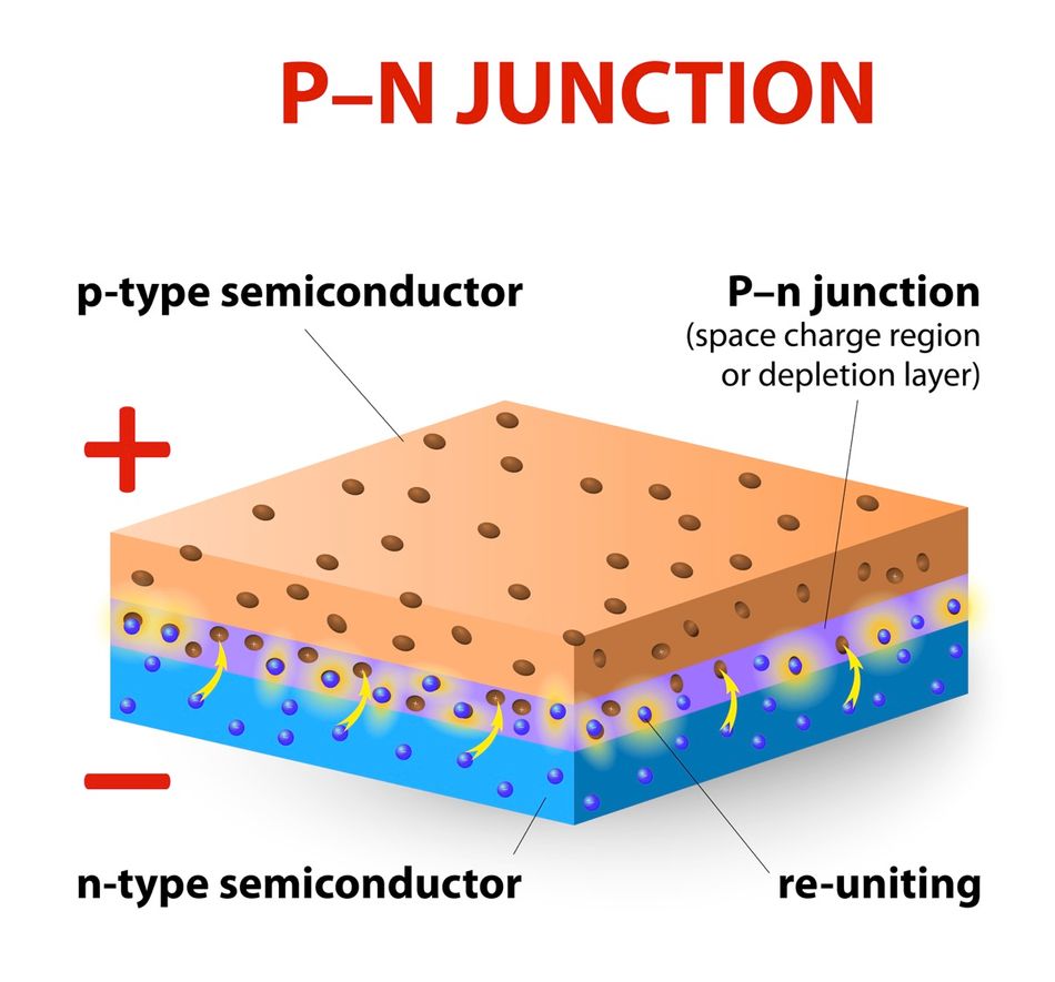
JFET is short for Junction Field-effect Transistor. It features a three-terminal structure i.e. drain, gate, and source. JFETs use a reverse-biased p-n junction to modulate channel conductivity, operating in depletion mode with a normally-on state.
There are two types of JFETs i.e.
N-channel JFETs
P-channel JFETs
JFETs excel in low-noise analog applications and high-temperature environments.
What are MOSFETs?
MOSFET is short for Metal Oxide Semiconductor Field Effect Transistor. It features an insulated gate structure with metal-oxide-semiconductor layers, offering both enhancement and depletion mode operations. These fundamental differences in gate structure and operation mechanism directly influence their application domains across analog circuits, power electronics, and integrated systems.
Hence, there are two main types of MOSFETs:
Enhancement type MOSFET
Depletion Type MOSFET
MOSFETs dominate digital electronics and high-power applications due to their superior switching characteristics and lower power dissipation. Understanding the technical nuances between these devices—from semiconductor physics to practical implementation considerations—enables engineers to optimize their designs for specific performance requirements, power constraints, and environmental conditions.
Semiconductor Physics and Operating Principles
The fundamental operation of both JFETs and MOSFETs relies on electric field-controlled charge carrier movement through a semiconductor channel.
How JFETs Work
In JFETs, the channel conductivity is modulated by varying the depletion region width through a reverse-biased p-n junction. The mathematical relationship governing the channel current can be expressed as:

Where;
IDSS represents the saturated drain current at zero gate voltage
VP is the pinch-off voltage
Hence, the current flowing from drain to source is directly proportional to the applied voltage.
Working of an N-Channel JFET
An N-type JFET consists of a semiconductor channel doped with n-type impurities, and a gate region doped with p-type impurities.
When a reverse bias voltage is applied to the gate, it depletes the channel of charge carriers, reducing the effective channel width and thus restricting the flow of current between the source and drain terminals.
Hence, the channel conductivity is controlled by varying the gate voltage, allowing for amplification or switching applications.
Working of a P-Channel JFET
P-channel JFET works similarly to an N-channel JFET but with opposite doping. It has a p-type semiconductor channel and an n-type gate.
When a reverse bias voltage is applied to the gate, it depletes the channel of majority charge carriers (holes), reducing the channel's conductivity.
However, P-channel JFETs generally have lower current-handling capabilities and slower switching speeds compared to N-channel JFETs.
Suggested Reading: Forward Bias, Reverse Bias and their effects on Diodes
How MOSFETs Work
MOSFETs utilize an insulated gate structure where the channel formation occurs through field-induced carrier accumulation or inversion. MOSFETs operate in three models i.e.
Linear model
Quadratic model
Variable Depletion layer model
The linear model describes the behavior of a MOSFET when it operates in the linear region. Hence, it can be considered as a linear device. In terms of electronic modeling, it can be replaced by a resistor which is modulated by the gate-to-source voltage.
The linear model is typically used for switching applications, digital signals and analog multiplication. The drain current equation is given as:

Where:
Qinv is the inversion layer charge per nuit area
W is gate width
L is gate length
tr is transit time
The quadratic model is similar to the linear model but it allows variation of inversion layer charge between source andd drain. Hence, it is modeled by the following equation:

The Varaible Depletion layer model accounts for the variation of charge in the depletion layer that exists between source and drain. It happens due to voltage variation along the channel.
How Enhancement Type MOSFETs Work
An enhancement-type MOSFET controls the flow of current source and drain by using an electric field applied to a third terminal (gate). When a voltage is applied to the gate, it attracts electrons to form a channel between the source and drain. This allows current to flow through the channel.
How Depletion Type MOSFETs Work
A depletion-type MOSFET controls the flow of source to drain current by depleting a channel of charge carriers. Unlike enhancement-type MOSFETs, depletion-type MOSFETs have a channel that is already present, and the gate voltage controls the width of this channel.
When a negative voltage (for an n-channel MOSFET) is applied to the gate, it repels the majority carriers in the channel, reducing its conductivity. This is known as the depletion mode.
Recommended Reading: PMOS vs NMOS: Unraveling the Differences in Transistor Technology
Technical Performance Analysis
Electrical Characteristics and Environmental Effects
The electrical characteristics of JFETs and MOSFETs exhibit distinct patterns across various operating parameters. DC characteristics show fundamental differences in device behavior:
Parameter | JFET | MOSFET |
Impedance (Z) | High, between megaohms to gigaohms | Higher, typically in gigaohms |
Transconductance (gm) | Lower, approx. 0.5 to 4 mS | Higher, approx. 1 to 20 mS |
The transconductance relationship follows:

AC performance metrics reveal significant operational differences:
Parameter | JFET | MOSFET |
Frequency Response | Typically lower, < 1 MHz | Higher, typically in MHz to GHz |
Switching Speed | Slower, up to 100 ns | Faster, < 20 ns |
Temperature characteristics demonstrate distinct behavioral patterns:
Parameter | JFET | MOSFET |
Temperature Coefficient | Negative, approx. -2 mV/°C | Positive, approx. +0.5 to +2.5 mV/°C |
Stability | Good temperature stability | Fair stability, can drift under high temp |
The temperature dependence of threshold voltage follows:

Noise performance metrics reveal crucial differences:
Parameter | JFET | MOSFET |
Noise Figure | Low noise figure, < 1 dB | Higher noise figure, approx. 2-3 dB |
1/f Noise | Lower levels of 1/f noise | Higher levels of 1/f noise |
The spectral noise density follows:

Where K is the flicker noise coefficient, f is frequency, k is Boltzmann's constant, T is temperature, and R is resistance.
Power Performance and Efficiency
Power handling capabilities between JFETs and MOSFETs differ significantly in terms of maximum ratings and operational efficiency. The total power dissipation follows the relationship:

Power Rating Parameter | JFET | MOSFET |
Maximum Power Dissipation | 0.5W - 2W | 1W - 250W |
Breakdown Voltage | 30V - 100V | 30V - 1500V |
Maximum Current | 10mA - 1A | 100mA - 100A |
Thermal characteristics significantly impact device performance:
Thermal Parameter | JFET | MOSFET |
Junction-to-Case Thermal Resistance | 15-40°C/W | 0.5-3°C/W |
Maximum Junction Temperature | 150°C | 175°C |
Safe Operating Area | Narrower | Wider |
Efficiency metrics reveal distinct operational characteristics:
Efficiency Metric | JFET | MOSFET |
On-State Resistance | Higher, 2-10Ω | Lower, 0.001-0.1Ω |
Switching Losses | Lower at high frequencies | Higher due to gate charge |
Power Efficiency | 85-90% | 90-98% |
The power loss during switching can be calculated using:

Design Implementation Guide
Application-Optimized Selection Framework
Device selection requires careful consideration of operating parameters and application requirements. The comprehensive selection matrix provides primary decision criteria:
Parameter | JFET | MOSFET | Selection Consideration |
Operating Voltage Range | 5V - 100V | 10V - 1500V | High voltage applications favor MOSFETs |
Maximum Current Rating | 1A - 10A | 100mA - 100A | Power applications require MOSFETs |
Gate Drive Voltage | Typically V_GS = 0 | 5V to 20V | Self-biased applications favor JFETs |
Switching Speed | Slow (< 1 MHz) | Fast (up to GHz) | Digital switching requires MOSFETs |
Thermal Resistance | High (15-40 °C/W) | Low (0.5-3°C/W) | Heat-critical designs favor MOSFETs |
Noise Performance | Low | Higher | Analog/audio applications favor JFETs |
Application Type | Analog | Digital/Analog | Application domain drives selection |
Operating Temperature Range | -55°C to 125°C | -55°C to 175°C | High-temperature applications favor MOSFETs |
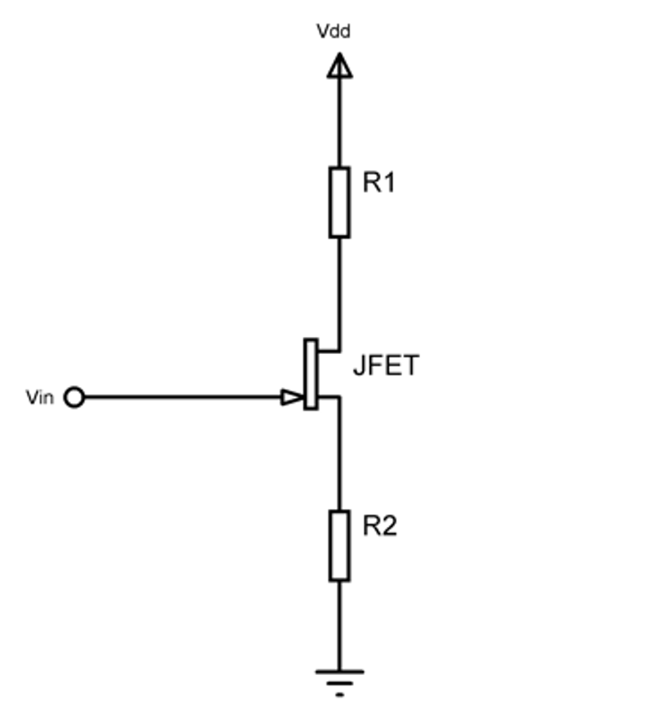
Common JFET source-follower configuration for analog applications:
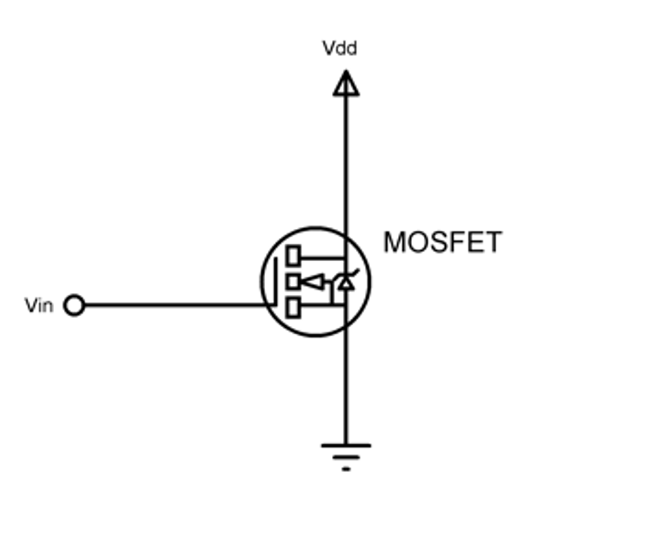
Basic MOSFET switching configuration:
Critical Design Trade-offs
The fundamental trade-offs between JFETs and MOSFETs impact device selection and implementation:
Parameter | JFET | MOSFET | Trade-off Implications |
Speed | Low speed, low power | High speed, moderate power | Requires careful design to avoid overheating |
Power | Good for low-power applications | Ideal for high-power applications | High drive losses at high speeds |
Noise and gain characteristics present crucial design considerations:
Parameter | JFET | MOSFET | Relationship Impact |
Noise | Low noise | Higher noise | Beneficial in low-noise applications |
Gain | Moderate gain levels | Higher gain potential | Critical in high-speed applications |
Reliability factors significantly influence long-term performance:
Factor | JFET | MOSFET |
Failure Rate | Low failure rates | Higher failure rates |
Thermal Variation Impact | Stable under thermal fluctuations | Sensitive to thermal stress |
Aging | Moderate aging effects | Less stable with age |
Design constraints require careful consideration:
Design Constraint | Considerations |
Temperature Limits | Keep below 125°C for JFETs |
Voltage Ratings | Ensure voltage ratings are 20% higher than operational |
Current Handling | Design for average current, not peak |
Integration Complexity | Simplicity is key for reliable designs |
Optimization strategies for enhanced performance:
Strategy | Description |
Proper Component Selection | Select components that match the desired specifications closely |
Thermal Management | Implement heat sinks or fans to dissipate heat effectively |
Circuit Topology Optimization | Design circuits to minimize parasitic elements and losses |
Use Cases and Applications
JFETs and MOSFETs address a variety of needs in the electronics design and manufacturing setup. Here are some of the application areas for both.
JFET Applications
High-Impedance Input Amplifiers
JFETs exhibit extremely high input impedance, making them ideal for amplifying signals from sources with high output impedance, such as microphones and other sensors.
Application: JFET input amplifiers are commonly used in audio preamplifiers, instrumentation amplifiers, and other circuits where minimal loading of the input source is critical.
Variable-Gain Amplifiers:
By varying the voltage applied to the gate of a JFET, its channel resistance can be controlled, thus adjusting the amplifier's gain.
Application: JFET-based variable-gain amplifiers are used in various applications, including audio equipment, radio receivers, and test instruments. This allows for dynamic adjustment of amplification levels, catering to different input signal strengths and desired output levels.
Suggested Reading: Selecting the Best Power Solution for Radio Frequency Signal Chain Phase Noise Performance
MOSFET Applications
Digital Logic Circuits
MOSFETs are the fundamental building blocks of digital circuits, including microprocessors, memory chips, and logic gates.
Example: In a simple inverter circuit, a MOSFET acts as a switch. When a high voltage is applied to the gate, the MOSFET turns on, allowing current to flow from the source to the drain, inverting the input signal. This principle is used to create complex logic gates like AND, OR, and NOT gates, which are the foundation of digital computers.
Power Electronics
MOSFETs are used in power electronics applications to efficiently control the flow of electrical power.
Example: In a DC-to-DC converter, MOSFETs are used as switches to convert a DC voltage level to another DC voltage level. This is essential in devices like laptop chargers and power supplies for electronic equipment. By rapidly switching the MOSFETs on and off, the converter can regulate the output voltage and current.
Conclusion
JFETs and MOSFETs serve distinct application domains with specific advantages. JFETs excel in low-noise, analog applications requiring stable thermal performance, while MOSFETs dominate high-power and high-speed digital applications. Device selection should prioritize application-specific requirements, considering thermal constraints, power requirements, and speed demands. Implementation success depends on careful consideration of operating conditions and proper thermal management.
Frequently Asked Questions
1. How do temperature variations affect device performance?
JFETs maintain stable performance up to 125°C with predictable behavior, while MOSFETs can operate at higher temperatures but require additional thermal management considerations.
2. What are the key considerations for high-frequency applications?
MOSFETs generally perform better in high-frequency applications due to lower input capacitance and faster switching speeds but require careful attention to gate drive design and layout considerations.
3. How can thermal management be optimized?
Implement proper heat sinking, ensure adequate airflow, and consider derating factors. For MOSFETs, special attention to thermal resistance from junction to case is crucial.
4. What are the critical factors for low-noise applications?
JFETs are preferred for low-noise applications due to their inherently lower noise characteristics. Consider bias point optimization and careful layout to minimize interference.