PVD vs CVD: Mastering Advanced Thin Film Deposition Techniques
This article delves into the core principles, process parameters, and material compatibility of PVD vs CVD, empowering researchers and engineers to make informed decisions for their advanced thin film endeavors.

17 Jul, 2024. 18 minutes read
Introduction
Thin film deposition is a cornerstone of modern materials engineering, enabling the creation of nanoscale coatings that revolutionize industries from electronics to aerospace. Physical Vapor Deposition (PVD) and Chemical Vapor Deposition (CVD) stand as the two primary techniques in this field, each offering unique capabilities for precise material manipulation. Both PVD vs CVD processes offer distinct advantages and find applications in diverse sectors, including solar cell production, medical implants, and cutting tools.
Understanding the fundamental differences between PVD vs CVD is crucial for selecting the optimal approach for a particular thin film deposition requirement. For material scientists and engineers, mastering these methods is crucial for advancing technology in semiconductors, optical coatings, and wear-resistant surfaces. This comprehensive article delves into the core principles, process parameters, and material compatibility of PVD vs CVD. Let’s start with the fundamentals…
The Fundamentals of PVD and CVD
Physical Vapor Deposition (PVD)
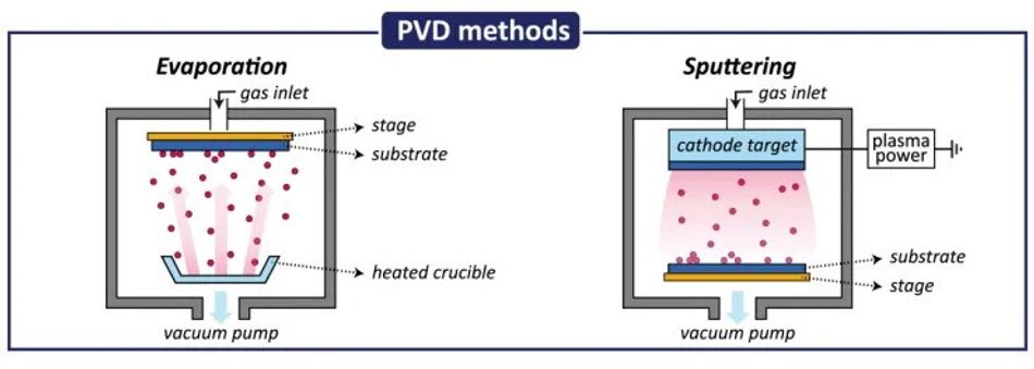
Physical Vapor Deposition (PVD) is a thin film deposition technique governed by thermodynamic principles, where solid materials are vaporized and transported through a vacuum or low-pressure gaseous environment to condense on a substrate. These thin films can be composed of various materials, including metals, alloys, ceramics, and even some polymers.
Here's a breakdown of the key aspects of PVD:
1. Material Transformation: In a PVD chamber, the target material (the material to be deposited) is transformed from its solid or liquid state into a vapor phase. This transformation can be achieved through several methods, most commonly:
Thermal Evaporation: The target material is heated to a high temperature using electrical resistance or electron bombardment, causing it to vaporize.
Sputtering: A high-energy plasma bombards the target material, ejecting atoms that transition into the vapor phase. [1]
Cathodic Arc Vaporization: A high current, low voltage arc is initiated between a cathode (target) and an anode. This arc creates a small, highly energetic spot on the cathode that vaporizes the target material at extremely high velocities.
2. Vacuum Environment: The PVD chamber is evacuated to a very low pressure (high vacuum). This minimizes collisions between the vaporized material and gas molecules, allowing for a more controlled and directed deposition process.
3. Transport and Deposition: The vaporized coating material travels through the vacuum chamber and condenses on the substrate, forming a thin film. The specific properties of the film, such as thickness, composition, and microstructure, depend on factors like the deposition rate, substrate temperature, and the distance between the target and substrate. Condensation occurs as the vapor particles strike the substrate surface, where surface diffusion and nucleation processes dictate film growth.
PVD encompasses several techniques, each with unique material removal and transport mechanisms:
Sputtering: Utilizes energetic ion bombardment to eject atoms from a target material.
Evaporation: Employs thermal energy to vaporize materials from a source.
Ion plating: Combines evaporation with concurrent ion bombardment of the growing film.
The main characteristics of PVD processes include:
Deposition Rates: Typically 1-10 nm/s for sputtering, 1-100 nm/s for evaporation.
Operating Pressures: 10-5 to 10-2 Torr for sputtering, 10-7 to 10-4 Torr for evaporation.
Energy Ranges: 1-10 eV for evaporation, 10-100 eV for sputtering
Plasma plays a crucial role in many PVD processes, particularly in sputtering and ion plating. It serves as a source of energetic ions and electrons, facilitating material removal from the target and enhancing film properties through ion bombardment. The plasma state, characterized by its high energy and reactivity, enables the ionization of sputtered or evaporated atoms, influencing their trajectory and energy upon reaching the substrate. This affects film structure and adhesion, overall.
Recommended Reading: PVD Coating in Semiconductors: A Comprehensive Guide
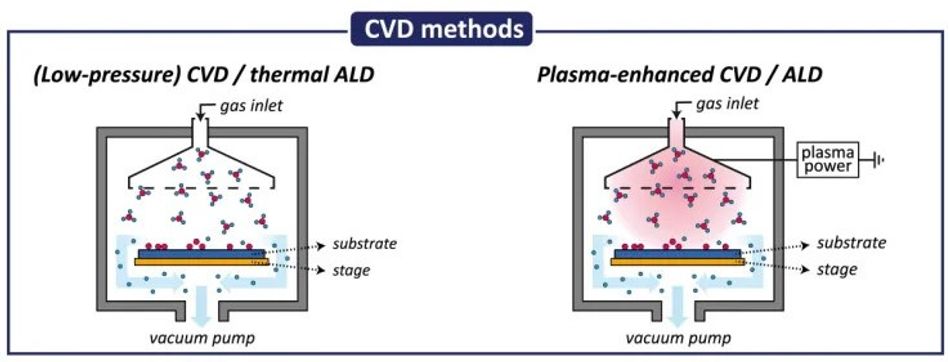
Chemical Vapor Deposition (CVD)
Chemical Vapor Deposition (CVD) is another thin film deposition technique fundamentally driven by chemical reactions occurring at the substrate surface. The process relies on the interplay between thermodynamics and kinetics to control the deposition of solid materials from gaseous precursors. Thermodynamics governs the driving force for reactions and determines the equilibrium state, while kinetics dictates the rate at which these reactions occur and influences the film growth mechanisms.
The primary stages of CVD include:
Precursors and Reactions: Volatile precursor molecules are introduced into the reaction chamber, often carried by an inert gas. Precursors undergo gas-phase reactions and/or surface reactions at the heated substrate, forming the desired thin film material. The selection of precursors is crucial, as they dictate the final film composition.
Activation Energy: To drive the chemical reactions, CVD often utilizes heat (thermal CVD) or plasma (plasma-enhanced CVD) to provide the necessary activation energy. This activation energy breaks down the precursor molecules and facilitates their reaction on the substrate.
Selective Deposition: A key advantage of CVD is its inherent selectivity. The chemical reactions are tailored to occur primarily on the substrate surface, minimizing unwanted film growth in the chamber.
Film Growth: The reaction byproducts are desorbed from the chamber using a vacuum pump, while the desired film material accumulates on the substrate, gradually building the thin film layer by layer.
CVD reactions typically involve complex mechanisms, including precursor decomposition, intermediate formation, and surface-catalyzed reactions. These processes can be described by detailed reaction pathways, often involving multiple steps and intermediates.
CVD encompasses several variants, each with unique chemistry and physics:
Plasma-Enhanced CVD (PECVD): Utilizes plasma to enhance chemical reactions, allowing for lower deposition temperatures. The plasma provides energy for precursor dissociation and can generate reactive species not accessible in thermal CVD. [2]
Metal-Organic CVD (MOCVD): Employs metal-organic compounds as precursors, enabling the deposition of compound semiconductors and other complex materials. The chemistry involves the decomposition of organometallic molecules and the subsequent reaction of metal and non-metal components.
Atomic Layer Deposition (ALD): A specialized form of CVD that uses self-limiting surface reactions to achieve atomic-scale thickness control. ALD relies on sequential, alternating exposure to different precursors, with each cycle depositing a single atomic layer.
Precursor chemistry plays a crucial role in CVD processes. The molecular structure of precursors influences their volatility, reactivity, and decomposition pathways. Ideal precursors exhibit high vapor pressure, clean decomposition, and appropriate reactivity. Common precursor types include halides, hydrides, and metal-organic compounds. The decomposition pathways of these precursors can involve β-hydride elimination, reductive elimination, or ligand exchange reactions, each affecting the resulting film composition and properties.
PVD can suffer from line-of-sight limitations, meaning only directly exposed surfaces receive the coating. CVD method, on the other hand, can create conformal coatings, covering even complex geometries. These deposition methods or coatings can be used to protect materials from corrosion.
Recommended Reading: Thin Film Deposition: Everything You Need to Know
Process Dynamics and Parameters
PVD Process Control and Optimization
PVD coating processes are governed by several critical parameters that significantly influence film properties and deposition rates. The primary parameters include:
Pressure: Typically ranging from 10-3 to 10-1 Pa, pressure affects mean free path and particle energy. Lower pressures generally result in higher particle energies and more directional deposition.
Temperature: Substrate temperature (usually 20-500°C) influences adatom mobility and film microstructure. The relationship between temperature (T) and surface diffusion coefficient (D) follows an Arrhenius-type equation:

Target Material: The choice of target material directly impacts film composition and properties. Sputter yield (Y) is related to incident ion energy (E) by Y ∝ En, where n typically ranges from 0.5 to 1 for most materials.
Power Density: Affects deposition rate (R) and is often linearly related: R ∝ P, where P is the power applied to the target.
The interplay of these parameters influences film properties such as density, stress, and microstructure. For instance, the film stress (σ) can be related to the ion-to-neutral ratio (i/n) and ion energy (Ei) by:

Advanced PVD techniques like High Power Impulse Magnetron Sputtering (HiPIMS) utilize high-power pulsed plasmas to achieve unique film properties. [3] In HiPIMS, peak power densities can reach 107 W/m², generating highly ionized plasmas. The pulse duration (typically 10-100 μs) and frequency (50-1000 Hz) control the plasma dynamics and ionization fraction.
Optimizing PVD processes for specific applications involves tailoring the ion-to-neutral ratio and energy distribution functions. Optimization techniques in PVD include:
Adjust working pressure to control mean free path and particle energies.
Optimize magnetic field configuration to enhance plasma confinement and ionization efficiency.
Utilize substrate bias to control ion bombardment energy and film stress.
Implement reactive gas flow control for stoichiometry management in compound films.
Fine-tune power and pulse parameters in HiPIMS to balance deposition rate and film quality.
By manipulating these parameters, engineers can achieve desired film properties such as density, adhesion, and microstructure for applications ranging from hard coatings to thin film electronics.
Recommended Reading: What is E-Beam Evaporation, and How Does it Compare to Other PVD Methods?
CVD Reaction Kinetics and Growth Mechanisms
Chemical Vapor Deposition (CVD) processes are governed by complex reaction kinetics and thermodynamics. The overall reaction rate is typically determined by the slowest step in the process, known as the rate-limiting step. This step can be mass transport-limited or surface reaction-limited, depending on process conditions. The reaction rate (R) follows an Arrhenius-type equation:

Where A is the pre-exponential factor, Ea is the activation energy, R is the gas constant, and T is the temperature. Activation energies for CVD processes typically range from 20 to 200 kJ/mol, depending on the specific reaction and rate-limiting step.
Growth mechanisms in CVD significantly influence film properties and can be categorized into three main types:
Island Growth (Volmer-Weber): Adatoms nucleate and grow as separate islands, eventually coalescing to form a continuous film. This mechanism often results in rougher surfaces and is common when adatom-adatom interactions are stronger than adatom-substrate interactions.
Layer-by-layer growth (Frank-van der Merwe): Adatoms preferentially attach to substrate edges, forming complete monolayers before initiating the next thin layer. This mechanism produces smoother films and occurs when adatom-substrate interactions are stronger than adatom-adatom interactions.
Mixed Growth (Stranski-Krastanov): Initial growth occurs layer-by-layer, followed by island formation. This mechanism is common in heteroepitaxial systems with lattice mismatch.
Surface mobility and nucleation theory play crucial roles in determining the dominant growth mechanism. Higher surface mobility generally promotes smoother films, while nucleation density affects grain size and film morphology.
Precursor chemistry and reactor design significantly impact CVD processes:
Precursor selection influences decomposition pathways, reaction rates, and film purity.
Reactor geometry affects gas flow dynamics, temperature gradients, and precursor distribution.
Boundary layer effects can limit mass transport to the substrate surface, influencing growth rates and uniformity.
CVD reaction equations can be complex, often involving multiple steps and intermediates. For example, the CVD of silicon from silane (SiH4) can be represented as: [4]
SiH4 (g) → Si (s) + 2H2 (g)
However, this overall reaction involves several elementary steps:
SiH4 (g) → SiH2 (g) + H2 (g) (Gas-phase decomposition)
SiH2 (g) → SiH2 (ads) (Adsorption)
SiH2 (ads) → Si (s) + H2 (g) (Surface reaction and desorption)
Side reactions and unwanted byproducts can significantly impact film quality. For instance, in the CVD of titanium nitride (TiN) using TiCl4 and NH3, the formation of solid NH4Cl can lead to particle contamination:
TiCl4 (g) + NH3 (g) → TiN (s) + 3HCl (g) + NH4Cl (s)
Understanding these reaction pathways and their kinetics is crucial for optimizing CVD processes and achieving desired film properties.
Recommended Reading: Magnetron Sputtering: A Versatile Thin Flim Deposition Technique
Head-to-Head: PVD vs CVD Comparison
Deposition Characteristics and Film Properties
Physical Vapor Deposition (PVD) and Chemical Vapor Deposition (CVD) exhibit distinct deposition characteristics and produce films with varying properties.
| Parameter | Physical Vapor Deposition | Chemical Vapor Deposition |
| Deposition Rate | 1 - 1000 nm/min | 1 - 10,000 nm/min |
| Film Uniformity | ±5 - 10% | ±1 - 5% |
| Substrate Temperature | 20 - 500°C | 200 - 1600°C |
| Operating Pressure | 105 to 10-2 Torr | 0.1 to 760 Torr |
| Step Coverage | Poor to Moderate | Excellent |
| Impurity Levels | <0.1% | 0.1 - 1% |
| Energy of Depositing Species | 1 - 100 eV | 0.1 - 1 eV |
Film microstructure, adhesion, and stress differ significantly between PVD and CVD deposited films:
Microstructure: PVD films often exhibit columnar grain structure with grain sizes ranging from 10-100 nm, while CVD films tend to have equiaxed grains with sizes from 50-500 nm. PVD films may show preferential crystallographic orientation due to directional deposition, whereas CVD films typically have more random orientations.
Adhesion: CVD generally provides better adhesion due to chemical bonding at the interface and higher deposition temperatures. PVD adhesion strength ranges from 10-100 MPa, while CVD can achieve 50-500 MPa. Interfacial reactions in CVD coating method can form graded compositions, enhancing adhesion.
Stress: PVD films often exhibit higher intrinsic stress (0.1-10 GPa) due to energetic particle bombardment. CVD films typically have lower stress (0.01-1 GPa) but can develop thermal stress during cooling from high deposition temperatures.
Unique advantages of Physical Vapor Deposition (PVD):
High-Quality Films: PVD enables the deposition of highly pure, dense, and adherent thin films with excellent uniformity.
Wide Material Compatibility: PVD can handle a vast array of materials, including those that decompose at higher temperatures (incompatible with CVD).
Precise Control: The process parameters in PVD allow for precise control over film thickness, composition, and microstructure.
Scalability: PVD can be scaled for both large-scale industrial applications and small-scale research projects.
Unique advantages of Chemical Vapor Deposition (CVD):
Precise Stoichiometry: CVD allows for the deposition of thin films with precise control over their elemental composition (stoichiometry). This is because the film composition directly reflects the chemical reactions between the precursors.
Conformal Coatings: CVD excels at creating conformal thin films, meaning the film uniformly coats even complex surface features of the substrate. This is due to the gaseous nature of the precursors, which can penetrate intricate geometries.
Low-Temperature Processing: Compared to PVD, CVD processes can often operate at lower temperatures. This makes them suitable for depositing thin films on heat-sensitive substrates that wouldn't withstand the high temperatures of some PVD methods.
Wide Range of Materials: CVD offers compatibility with a vast array of materials, including elements, compounds, and even certain polymers. This versatility allows for the creation of thin films with diverse properties.
By understanding the deposition characteristics and resulting film properties of PVD vs CVD, engineers can make informed decisions for their specific thin film coating needs. This paves the way for advancements in diverse fields like microelectronics, optics, and photovoltaics.
Recommended Reading: Conformal Coating Process: Protecting Electronics in Harsh Environments
Advanced Applications and Emerging Trends
Application-Specific Performance
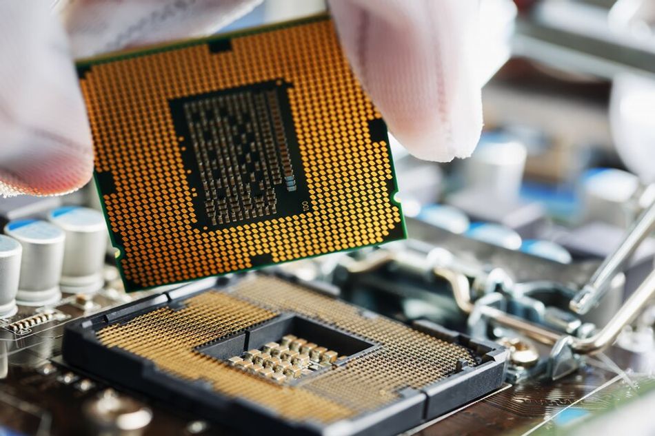
The choice between Physical Vapor Deposition and Chemical Vapor Deposition is highly dependent on the specific application requirements and the unique advantages each technique offers. In the semiconductor industry, both methods play crucial roles but in different domains. PVD is the go-to technique for metal contacts and interconnects, particularly for materials like aluminium and copper. Its ability to operate at relatively low temperatures (below 400°C) while maintaining high purity levels makes it ideal for applications where thermal budgets are tight and contamination is minimized.
Conversely, CVD dominates in the deposition of dielectric layers such as silicon dioxide (SiO2) and silicon nitride (Si3N4). It also excels in the epitaxial growth of semiconductors. The key advantage of CVD in these applications is its superior conformality, often achieving step coverage greater than 95%, and its precise control over stoichiometry. This makes CVD indispensable for creating uniform insulating layers and high-quality crystalline structures essential in advanced semiconductor devices.
In the realm of optical coatings, both techniques find their niches. PVD shines in the production of precision optical filters and anti-reflective coatings. Its strength lies in its ability to provide exceptionally accurate thickness control, often within ±1 nm, and achieve very low absorption rates (less than 0.1%). These characteristics are crucial for high-performance optical components. On the other hand, CVD proves its worth in large-area applications, such as low-emissivity (low-E) glass coatings. Here, CVD's high throughput capabilities (over 100 m²/h) and good uniformity (typically ±2% over a 3x3 m² area) make it the preferred choice for industrial-scale production.
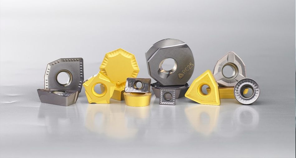
The wear-resistant coatings field showcases another aspect of the PVD-CVD dichotomy. PVD excels in creating hard coatings like titanium nitride (TiN) and chromium nitride (CrN) for cutting tools. These coatings boast impressive hardness values ranging from 20 to 40 GPa and low friction coefficients between 0.1 and 0.5, significantly enhancing tool life and performance. CVD, meanwhile, finds its strength in producing thick (over 10 µm) diamond-like carbon (DLC) coatings, particularly valuable in automotive components. These CVD-deposited DLC coatings offer exceptional wear resistance, with wear rates often below 10-7 mm³/Nm, contributing to improved efficiency and longevity of mechanical parts.
Geometry also plays a crucial role in technique selection. When coating complex 3D structures, CVD's superior conformality becomes a significant advantage. It can achieve over 90% step coverage in features with aspect ratios as high as 10:1, far outperforming PVD, which typically struggles to reach 50% coverage in similar structures. However, when ultra-high purity is the primary concern, PVD often takes the lead, capable of achieving impurity levels below 10 parts per million (ppm), compared to CVD's typical range of 100-1000 ppm.
These characteristics translate into diverse industrial applications. In aerospace, PVD is crucial for creating thermal barrier coatings on turbine blades, depositing materials like yttria-stabilized zirconia (YSZ) in layers 100-500 µm thick, with thermal conductivity below 1 W/mK. The electronics industry relies heavily on PVD for thin film metallization in integrated circuits, creating multi-layer structures like Ti/TiN/AlCu with thicknesses below 1 µm and resistivities under 3 µΩ·cm. [6]
CVD, meanwhile, is a cornerstone technology in the solar industry, used for depositing silicon in photovoltaic cells. It can create amorphous silicon (a-Si:H) layers 1-2 µm thick with conversion efficiencies exceeding 15%. In tool manufacturing, CVD is essential for producing tungsten carbide coatings on cutting inserts, creating WC-Co layers 5-15 µm thick with hardness values over 2000 HV.
In conclusion, the choice between PVD and CVD is rarely straightforward and depends on a complex interplay of factors. Understanding these nuances is crucial for engineers and materials scientists to ensure the best possible performance and efficiency in diverse technological fields.
Innovations in CVD Technology
Chemical Vapor Deposition (CVD) technology has undergone significant advancements, with Atomic Layer Deposition (ALD) and Plasma-Enhanced CVD (PECVD) emerging as groundbreaking variants. ALD utilizes sequential, self-limiting surface reactions to achieve atomic-scale thickness control. Its unique reaction mechanism involves alternating exposure to precursors, with each cycle depositing a single atomic layer. This allows for unprecedented precision in film thickness (±0.1 Å) and conformality (>99% in 100:1 aspect ratio structures). Process control in ALD relies on the precise timing of precursor pulses and purge steps, typically in the millisecond range.
PECVD employs plasma to enhance chemical reactions, enabling deposition at lower temperatures (100-350°C) compared to thermal CVD. The plasma provides energy for precursor dissociation, generating reactive species not accessible in thermal processes. This allows for the deposition of materials like silicon nitride at 300°C instead of the 700-800°C required in thermal CVD. Process control in PECVD involves managing plasma parameters such as power density (0.1-1 W/cm²) and frequency (13.56 MHz or 2.45 GHz).
CVD has played a crucial role in the synthesis of advanced materials like graphene and carbon nanotubes (CNTs). For graphene growth, CVD typically uses methane as a carbon source on copper substrates at temperatures around 1000°C. The process can produce large-area, high-quality graphene with carrier mobilities exceeding 10,000 cm²/Vs. [5] CNT growth via CVD employs catalysts like iron nanoparticles and carbon sources such as ethylene or acetylene at temperatures between 600-1200°C. This method can produce single-walled CNTs with diameters as small as 0.7 nm and lengths up to several centimeters.
In next-generation semiconductor manufacturing, CVD faces the challenge of conformal deposition in high-aspect-ratio structures. As feature sizes shrink below 5 nm, traditional CVD struggles to achieve uniform coverage in deep trenches and vias. ALD has emerged as a solution, capable of depositing uniform films in structures with aspect ratios exceeding 100:1. However, the inherently slow deposition rate of ALD (typically 0.1-0.2 nm/cycle) presents throughput challenges.
Innovations like spatial ALD, which separates precursors spatially rather than temporally, aim to increase deposition rates to >1 nm/s while maintaining ALD's precision.
These advancements in CVD technology are transforming various industries:
Microelectronics: Enabling the creation of ultra-thin gate oxides and other critical components for ever-shrinking transistors in modern microchips.
Photovoltaics: Developing high-efficiency solar cells with improved light absorption and charge transport properties.
Microfluidics: Creating microfluidic channels and devices with precise geometries and surface functionalities for applications in bioanalysis and diagnostics.
Sensors: Depositing functional thin films for highly sensitive and selective gas sensors or biosensors.
The future of CVD lies in pushing the limits of miniaturization, achieving even greater control over film properties, and exploring the deposition of novel materials with groundbreaking functionalities.
Hybrid and Complementary Techniques
Hybrid deposition techniques combining elements of Physical Vapor Deposition (PVD) and Chemical Vapor Deposition (CVD) have emerged to leverage the strengths of both methods. One such technique is Plasma-Enhanced Chemical Vapor Deposition (PECVD) with ion bombardment. This utilizes plasma to enhance chemical reactions while incorporating energetic ion bombardment typical of PVD processes. This synergistic approach allows for lower deposition temperatures (200-400°C) compared to thermal CVD while achieving improved film density and adhesion characteristics of PVD.

Another hybrid method is High Power Impulse Magnetron Sputtering (HiPIMS) combined with PECVD. This technique uses high-power, short-duration pulses to create a highly ionized metal vapor, which is then reacted with gaseous precursors in a plasma environment. The result is enhanced control over film composition and microstructure, with the ability to deposit dense, low-stress films at lower temperatures than conventional magnetron sputtering or thermal CVD.
These hybrid methods overcome the limitations of individual PVD and CVD processes. For instance, the PECVD with ion bombardment technique addresses the poor step coverage of traditional PVD while maintaining the low-temperature deposition capability. It can achieve step coverage of >90% in features with aspect ratios up to 10:1, compared to <50% for conventional PVD. The HiPIMS-PECVD combination overcomes the low ionization efficiency of standard magnetron sputtering (typically <5%) by achieving metal ionization rates of >50%, leading to improved film adhesion and the ability to tailor film stress from compressive to tensile (-2 GPa to +1 GPa).
Complementary techniques are often used in conjunction with PVD or CVD to enhance film properties. Ion implantation, for example, can be employed post-deposition to modify the near-surface region of PVD or CVD films. In the case of TiN coatings deposited by PVD, nitrogen ion implantation (dose: 1x10¹⁷ ions/cm², energy: 100 keV) can increase surface hardness from 20 GPa to 35 GPa and improve wear resistance by a factor of 2-3.
Annealing is another crucial complementary technique. For CVD-deposited high-k dielectric films like HfO2, post-deposition annealing in N2 at 800-1000°C for 30-60 seconds can reduce defect density by an order of magnitude (from 1012 to 1011 cm-2) and increase the dielectric constant from 18 to 22.
Complex multilayer coatings often utilize both PVD and CVD to achieve optimal performance. A prime example is the multilayer coating used in cutting tools:
PVD TiN Base Layer (1-2 µm): Provides excellent adhesion to the substrate and a smooth surface for subsequent layers.
CVD Al2O3 Intermediate Layer (2-4 µm): Offers superior hot hardness and oxidation resistance.
PVD TiAlN Top Layer (1-2 µm): Provides high hardness and low friction coefficient.
This combination leverages the high adhesion and smooth surface of PVD TiN, the excellent hot hardness and chemical stability of CVD Al2O3, and the superior wear resistance of PVD TiAlN. The resulting coating exhibits a tool life increase of 200-300% compared to single-layer coatings, with the ability to maintain hardness >30 GPa at temperatures up to 1000°C.
Recommended Reading: Ultra-Precise Deposition for the Fabrication of Next-Generation MicroLED and QD-LED Displays
Conclusion
PVD and CVD offer distinct strengths for thin film deposition. PVD shines in precise control and low-temperature processing, while CVD excels in conformality and deposition rate. Understanding the underlying physics and chemistry of both processes empowers engineers to make informed decisions for specific applications. Future advancements like hybrid PVD-CVD processes and atomic-scale engineering hold immense promise for creating novel materials and devices, propelling innovation across diverse technological frontiers.
Frequently Asked Questions
Q: How does one determine the optimal ion-to-neutral ratio in HiPIMS for a specific application?
A: The optimal ion-to-neutral ratio in HiPIMS depends on the desired film properties and typically ranges from 30-70%. It can be controlled by adjusting pulse parameters such as peak power density (0.5-10 kW/cm²) and pulse duration (50-200 µs). Experimentation using Langmuir probe measurements and correlating results with film properties (e.g., stress, density) is crucial for optimization.
Q: What strategies can be employed to mitigate particle formation in PECVD of silicon nitride?
A: Particle formation in PECVD of silicon nitride can be mitigated by:
Optimizing gas ratios (e.g., SiH4:NH3 ratio of 1:5 to 1:10)
Using pulsed plasma with duty cycles of 10-50%
Implementing substrate biasing (-50 to -200 V) to repel negatively charged particles
Increasing chamber pressure (1-5 Torr) to reduce gas-phase nucleation
Employing in-situ plasma cleaning between deposition cycles
Q: How can one achieve conformal coating of high-aspect-ratio (>100:1) nanostructures?
A: Conformal coating of high-aspect-ratio nanostructures can be achieved using:
Atomic Layer Deposition (ALD) with optimized precursor exposure and purge times
Supercritical fluid deposition using CO2 as a carrier for precursors
Molecular Layer Deposition (MLD) for organic or hybrid organic-inorganic coatings
Initiated CVD (iCVD) for polymer coatings These techniques can achieve >95% step coverage in structures with aspect ratios exceeding 1000:1.
Q: How can one optimize PVD processes for the deposition of high-entropy alloy (HEA) thin films?
A: Optimizing PVD for HEA thin films involves precise control of parameters like sputter power (for uniform composition) and substrate temperature (to manage stress and crystallinity). In-situ monitoring and material selection for compatible targets are also crucial for achieving high-quality HEA films.
Q: What are the latest developments in in-situ monitoring and control of thin film growth?
A: Recent advancements in in-situ monitoring include real-time characterization using techniques like x-ray photoelectron spectroscopy (XPS) and spectroscopic ellipsometry. These offer deeper insights into film composition and growth dynamics. Additionally, machine learning algorithms are being explored for real-time process control, enabling automatic adjustments for optimized film properties.
References
[1] Wevolver. PVD Coating in Semiconductors: A Comprehensive Guide [Cited 2024 July 15] Available at: Link
[2] OXINST. Plasma Enhanced Chemical Vapour Deposition (PECVD) [Cited 2024 July 15] Available at: Link
[3] ResearchGate. Principles of Vapor Deposition of Thin Films [Cited 2024 July 15] Available at: Link
[4] ScienceDirect. Simulation of SiC Deposition from SiH4/C3H8/Ar/H2 Mixtures in a Cold Wall CVD Reactor [Cited 2024 July 15] Available at: Link
[5] NCBI. Chemical Vapour Deposition of Graphene—Synthesis, Characterisation, and Applications: A Review [Cited 2024 July 15] Available at: Link
[6] NCBI. PVD Coating vs CVD Coating: 8 Important Things to Consider [Cited 2024 July 15] Available at: Link
Table of Contents
IntroductionThe Fundamentals of PVD and CVDPhysical Vapor Deposition (PVD) Chemical Vapor Deposition (CVD) Process Dynamics and ParametersPVD Process Control and OptimizationCVD Reaction Kinetics and Growth MechanismsHead-to-Head: PVD vs CVD ComparisonDeposition Characteristics and Film PropertiesAdvanced Applications and Emerging TrendsApplication-Specific PerformanceInnovations in CVD TechnologyHybrid and Complementary TechniquesConclusionFrequently Asked QuestionsReferences