Single Sided PCB: A Comprehensive Guide
In this comprehensive guide, we will explore the design, manufacturing process, advantages, and limitations of single sided PCBs, helping you understand their critical role in modern electronics.
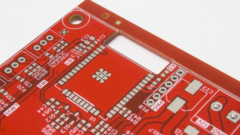
Single Sided PCB with Solder Mask and Surface Mount Components
Introduction
Single Sided PCBs (Printed Circuit Boards) are the simplest and most cost-effective type of PCB widely used in various electronic applications. Featuring a conductive layer on only one side of the board, these PCBs are ideal for designs requiring minimal complexity. From consumer electronics to industrial controls, single sided PCBs provide an efficient solution for straightforward circuitry needs.
The structure of a single sided PCB includes a copper layer for electrical connections and a substrate for mechanical support. This design makes them a preferred choice for high-volume production due to their affordability and ease of manufacture. Additionally, single sided PCBs are highly versatile, finding applications in LED lighting, power supplies, and household appliances.
This article presents the essential features of single-sided PCBs, explaining their role in modern electronics!
What is a Single Sided PCB?
Definition and Core Components
A single-sided PCB (Printed Circuit Board) is a type of circuit board that contains only one layer of conductive material. [1] This copper layer serves as the medium for forming electrical connections between the electronic components mounted on the PCB. Unlike multilayer PCBs, which have multiple conductive layers separated by insulating material, single-sided PCBs concentrate all circuits and components on a single layer. This makes them ideal for low-cost, low-density applications that do not require intricate routing or high-speed signal integrity.
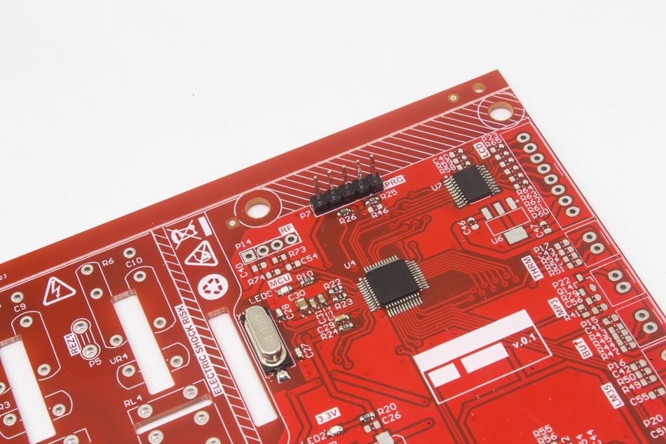
Core Components of a Single-Sided PCB
A single-sided PCB consists of several key components that work together to form the functional circuit:
Substrate: The base material, providing mechanical strength and electrical insulation, is usually made of FR-4 (fibreglass), phenolic resin, or epoxy-based composites. The choice of material depends on the application, with FR-4 offering higher durability and resistance to thermal stress.
Copper Layer: A thin conductive layer of copper foil, typically with a copper thickness ranging from 1 to 3 ounces per square foot, is laminated onto the substrate. This layer creates the electrical pathways necessary for current flow.
Solder Mask: A protective epoxy-based coating applied over the copper traces to prevent oxidation, solder bridging, and short circuits during assembly. It also gives the PCB it's characteristic green, red, or blue color.
Silkscreen: A printed overlay containing component identifiers, polarity markers, and logos for easier assembly, troubleshooting, and debugging. The silkscreen is often made from epoxy ink and applied using screen printing or other advanced techniques.
Differences Between Single Sided and Multilayer PCBs
Single-sided and multilayer PCBs differ significantly in terms of construction, cost, and applications. For example, single-sided PCBs are often used in simple devices like calculators and LED lighting systems, while multilayer PCBs are essential for advanced electronics such as smartphones and high-performance computing devices.
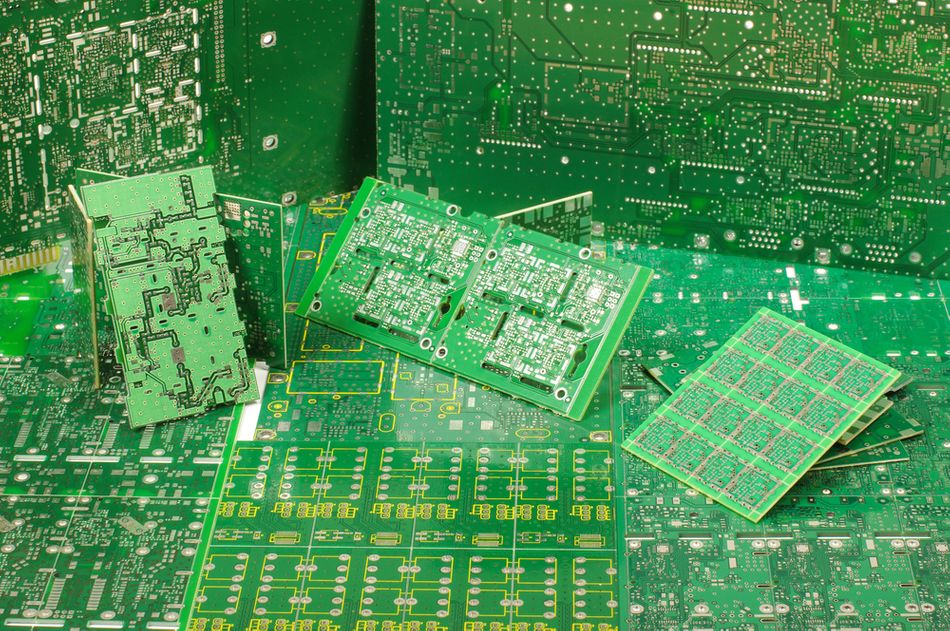
A single-sided PCB consists of a single layer of conductive material, while multilayer PCBs have multiple conductive layers separated by insulating materials. [2] The simpler design of single-sided PCBs makes them less expensive and easier to manufacture, whereas multilayer PCBs can handle more complex circuits and higher component densities.
Let’s go through their basic differences:
| Feature | Single-Sided PCBs | Multilayer PCBs |
| Construction | Single Conductive Layer | Multiple Conductive Layers |
| Cost | Low | High |
| Applications | Simple, Low-Density Circuits | Complex, High-Density Circuits |
| Design Complexity | Easy to Design | Requires Advanced Design Techniques |
| Manufacturing | Straightforward and Quick | Time-Consuming and Challenging |
Single-sided PCBs are typically used for low-cost devices with straightforward routing requirements. They are suitable for applications like power supplies, calculators, and simple SMD assemblies. Multilayer PCBs enable complex stackup designs with higher component density and signal integrity. They are commonly used in applications demanding high-quality performance, such as critical infrastructure systems and high-speed computing.
Single Sided PCBs remain indispensable in the electronics industry, where simplicity and affordability outweigh the need for handling complex circuits. They continue to play a pivotal role in PCB assembly for consumer products and industrial use cases.
Recommended Reading: Types of Printed Circuit Boards: A Comprehensive Guide
Manufacturing and Design Techniques for Single Sided PCBs
Overview of the Manufacturing Process
The manufacturing process of a single-sided PCB involves several critical steps to ensure quality and functionality.
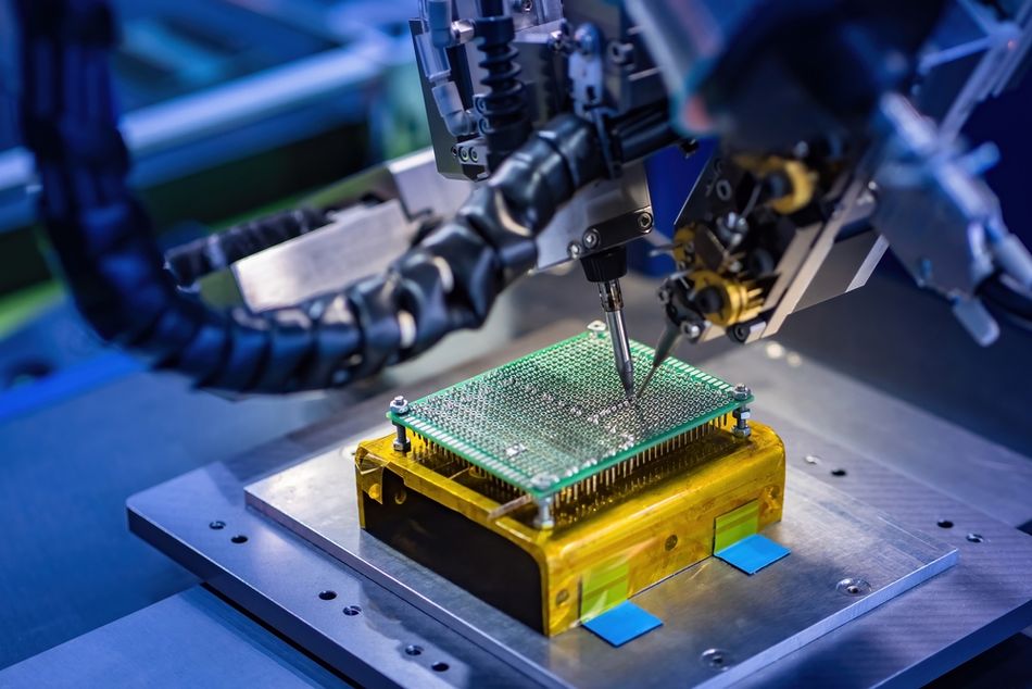
Below is a step-by-step guide:
Substrate Preparation: This step ensures that the base material is free of impurities and properly sized, which is essential for achieving a clean surface for copper lamination. The base material, typically FR-4 or phenolic resin, is cleaned and cut to the required dimensions. [3]
Copper Patterning: A thin copper layer is laminated onto the substrate. The desired circuit pattern is created using photoresist coating and ultraviolet light exposure. Unwanted copper is etched away using a chemical solution.
Drilling: Holes for component leads are drilled using precision equipment to ensure accurate placement.
Solder Mask Application: A protective layer of solder mask is applied to the board to prevent oxidation and accidental soldering of unintended areas.
Final Testing: The board undergoes electrical testing to verify circuit continuity and functionality. Quality control checks ensure all specifications are met.
Below are some advanced techniques for enhanced manufacturing:
Surface Finish: Processes like ENIG (Electroless Nickel Immersion Gold) can be applied for corrosion resistance and improved solderability.
Copper Thickness Adjustment: Custom copper thickness can be selected based on the current carrying requirements of the board.
Epoxy Coatings: High-quality epoxy is often used for additional structural integrity and thermal resistance.
The streamlined and cost-effective manufacturing process of single-sided PCBs makes them an excellent choice for applications like LED lighting, calculators, and basic electronic devices.
Design Considerations
Designing single-sided PCBs involves addressing several key factors to ensure optimal performance and manufacturability. Proper layout optimization and thermal management are crucial to achieving reliable designs.
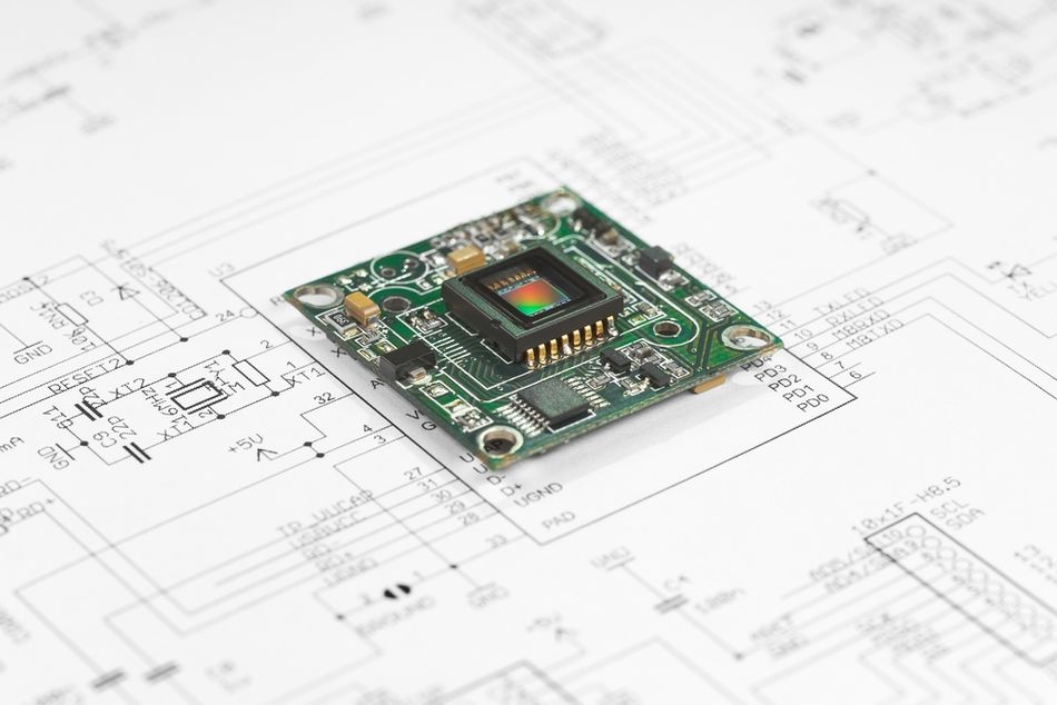
Below are key considerations and best practices:
Layout Optimization:
Efficiently arrange components and routing to minimize signal interference and ensure a logical flow of connections.
Avoid crossing traces, which is especially critical for single-sided PCBs with limited routing flexibility.
Maintain adequate spacing between traces to meet electrical safety and PCB manufacturing standards.
Thermal Management:
Prevent overheating by incorporating heat sinks, thermal pads, or base materials with high thermal conductivity.
Place heat-generating components strategically to distribute heat evenly and avoid thermal hotspots.
For high-power applications like power supplies, ensure sufficient trace width and thickness to handle current loads effectively.
Tips for Using PCB Design Software
Designing single-sided PCBs with PCB design software requires leveraging its features to create efficient and error-free layouts. Below are some practical tips to optimize your design process and ensure high-quality outcomes:
Auto-Routing Features: Utilize auto-routing to speed up design processes, but manually adjust critical traces for signal integrity and performance.
Design Rule Checks (DRC): Leverage built-in DRC tools to detect and correct potential issues, such as inadequate spacing, incorrect copper thickness, or trace width mismanagement.
Thermal and Electrical Simulations: Simulate thermal behavior and electrical performance to identify potential challenges. They use simulation tools to optimize circuit design, ensuring balanced current distribution and effective heat dissipation.
Common Design Pitfalls and Solutions
Designing single-sided PCBs can present unique challenges due to limited routing space and the constraints of having a single conductive layer. Below are common pitfalls encountered during the design process and practical solutions to overcome them:
Overcrowded Layouts:
Issue: Placing components too close can cause short circuits and hinder soldering.
Solution: Increase spacing and prioritize high-frequency or power-critical paths.
Trace Width Mismanagement:
Issue: Traces that are too thin for high-current applications lead to overheating and possible failures.
Solution: Use trace width calculators to size traces according to current capacity and thermal constraints.
Inefficient Grounding:
Issue: Poor grounding introduces noise and signal instability.
Solution: Design a continuous ground plane or wide grounding traces to improve signal integrity and noise reduction.
Advanced Design Enhancements
To maximize the performance, reliability, and versatility of single-sided PCBs, designers can implement advanced techniques and enhancements. While these boards are inherently simpler than multilayer designs, employing innovative methods can help overcome their limitations and expand their application potential.
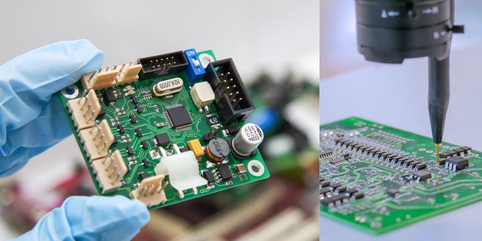
Below are some advanced design enhancement techniques:
Solder Mask Optimization: Ensure the solder mask covers all non-soldered areas to prevent oxidation and accidental shorts.
Single Layer PCB Challenges: Address the inherent limitations of a single-layer board by using advanced routing strategies and stackup considerations when transitioning to double-sided boards.
Ground and Power Planes: Implement solid grounding techniques, even in single-sided designs, by using wide copper areas for grounding.
With proper design techniques and an understanding of potential pitfalls, single-sided PCBs can meet the demands of low-cost, low-density designs while maintaining reliability in their applications.
Recommended Reading: PCB Design: A Comprehensive Guide to Printed Circuit Board Design
Applications of Single Sided PCBs in Electronics
Key Applications
Single-sided PCBs are widely used in various industries due to their simplicity and cost-effectiveness.
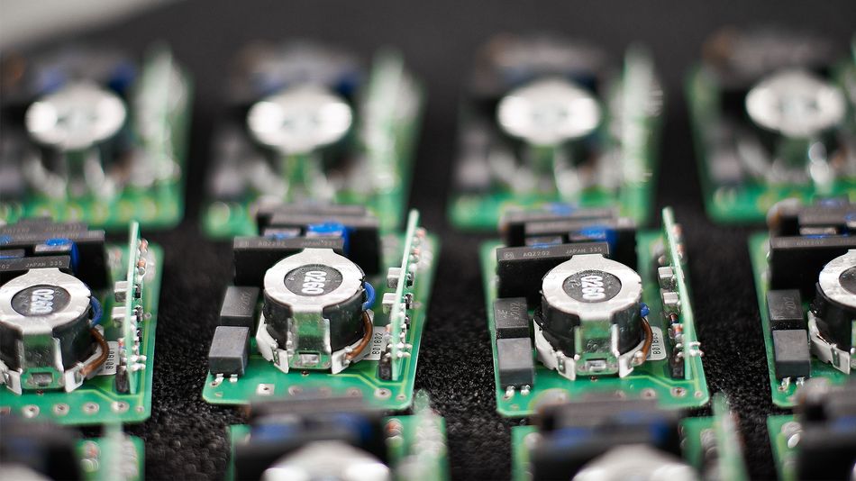
For example, in consumer electronics, their straightforward design allows for low-cost production of items like calculators and remote controls. In lighting systems, single-sided PCBs are particularly effective in supporting LED technologies, ensuring efficient energy use while keeping costs low. Their straightforward design and ease of manufacturing make them suitable for numerous applications, especially those requiring low-density circuits. Below are some of the most common use cases:
Consumer Electronics: Found in devices such as calculators, remote controls, and basic audio equipment.
Lighting Systems: Commonly used in LED boards and lighting panels for residential and commercial purposes.
Industrial Controls: Ideal for simple relay circuits and control panels.
Power Supplies: Frequently utilized in low-power adapters and chargers.
The single conductive layer simplifies the design and reduces manufacturing complexity, enabling faster PCB production times and lower costs compared to multilayer alternatives.
Why Single-Sided PCBs Stand Out?
Single-sided PCBs stand out primarily due to their simplicity and cost-effectiveness. Here's a breakdown of their key advantages:
Cost-Effectiveness:
The reduced complexity of single-sided PCBs translates to lower PCB manufacturing costs, making them highly economical for high-volume production.
Ease of Manufacturing:
The absence of multilayer stack-ups or lamination processes enables faster production and reduces the potential for manufacturing defects.
Reliability for Simpler Designs:
For applications requiring basic circuitry, such as SMD or through-hole components, single-sided PCBs provide a robust solution with fewer points of failure.
The versatility and cost-effective nature of single-sided PCBs continue to drive their widespread adoption in industries where affordability and simplicity are top priorities.
Advantages and Limitations
Single-sided PCBs offer several significant advantages due to their simple design and manufacturing process. These boards are highly cost-effective, making them suitable for budget-conscious projects. Their straightforward structure enables quick and efficient production, ensuring reliability in applications with low complexity requirements.
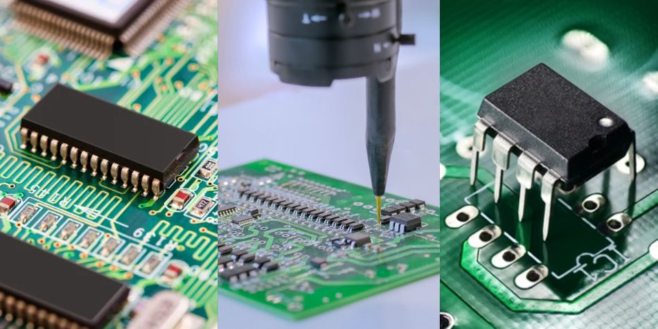
However, single-sided PCBs come with limitations, primarily due to their reduced complexity and lower circuit density. They cannot accommodate advanced or high-density designs, limiting their use to simpler applications.
Let’s go through this comparison table:
| Aspect | Advantages | Limitations |
| Cost | Low Cost Manufacturing | Not Suitable for High-End Applications |
| Design Complexity | Simple, Easy to Design | Limited to Low Complexity Circuits |
| Circuit Density | Ideal for Low-Density Circuits | Insufficient for Complex, Multi-Layered Needs |
| Manufacturing | Quick and Efficient | Cannot Support Advanced Manufacturing Techniques |
While single-sided PCBs are excellent for cost-effective and simple designs, they are not suitable for applications requiring advanced performance or high circuit density. Understanding these trade-offs is essential when selecting a PCB type for your project. For higher complexity needs, transitioning to double-sided boards or multilayer PCBs may be necessary.
Recommended Reading: SMT VS SMD (VS THT): A Comprehensive Guide to Electronics Assembly Techniques
Challenges in Working with Single Sided Boards
Design Challenges
Designing single-sided PCB boards requires careful consideration due to the limited space for routing and the absence of multiple conductive layers. These limitations often lead to increased design complexity and require creative solutions to achieve an optimized layout.
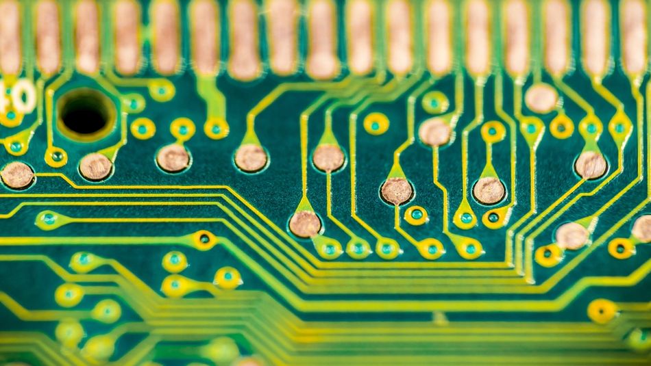
Below are some major design challenges:
Space Constraints:
With all traces and electronic components on a single side, maintaining adequate spacing between traces becomes difficult.
Overlapping traces can result in signal interference, short circuits, or inefficient layouts.
Trace Routing:
All connections must fit within the single conductive layer or vias, making routing intricate and time-consuming.
Crossing paths is not an option, so designers must use creative PCB layouts to avoid bottlenecks in high-density designs.
Component Placement:
Poor placement can lead to extended trace lengths, increasing resistance and reducing performance.
Thermal management becomes challenging, especially for heat-generating components like power transistors and LEDs.
Practical Tips to Address Design Challenges
Compact Layouts:
Arrange components strategically to minimize trace lengths and avoid overlaps.
Use PCB design software to explore multiple configurations and achieve a balanced layout.
Optimize Trace Routing:
Employ diagonal or curved traces to maximize space utilization and improve signal paths.
Utilize routing algorithms in design tools to automate trace optimization while adhering to design rules.
Simulate and Validate Designs:
Perform electrical and thermal simulations using tools like SPICE and thermal analysis software to detect potential issues.
Use Design Rule Checks (DRC) to ensure compliance with manufacturing constraints.
Manufacturing Challenges
Manufacturing single-sided PCBs comes with several challenges. Achieving precise etching is critical for maintaining the integrity of circuit paths, but inconsistencies in the etching process can lead to short circuits or open circuits. Thermal performance is another significant concern, as single-layer designs lack the advanced thermal dissipation features found in multilayer boards.
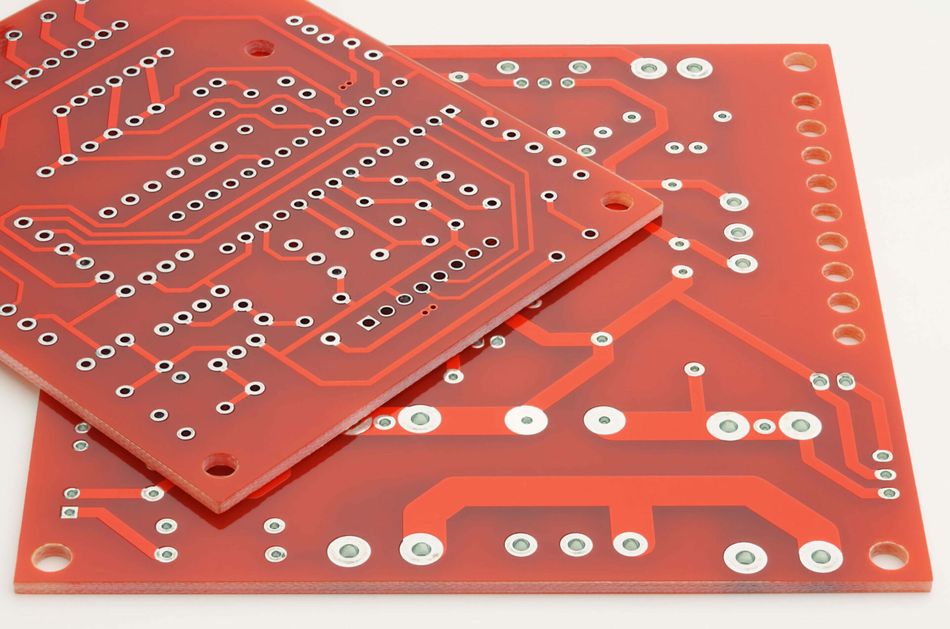
Below are key manufacturing challenges:
Precise Etching:
Variability in the etching process can lead to incomplete removal of unwanted copper, resulting in short circuits or open circuits.
Thin traces are particularly susceptible to over-etching, compromising the circuit design.
Thermal Performance:
Without multiple layers to spread heat, single-sided PCBs are prone to thermal buildup.
Overheating can damage components or degrade overall system reliability.
Inspection and Quality Control:
Defects in single-layer designs, such as misaligned traces or pinholes in the solder mask, can be challenging to detect visually.
Solutions to Overcome Manufacturing Challenges
Precision Etching:
Utilize high-quality photoresists and controlled etching solutions like ferric chloride for consistent results.
Adopt advanced computer-aided manufacturing (CAM) tools to ensure accurate trace patterning.
Thermal Management:
Incorporate heat sinks, thermal pads, or copper pours to distribute heat effectively.
Use thicker copper layers (e.g., 2 oz/sq ft) for improved current carrying and thermal dissipation. [4]
Advanced Tools and Processes:
Employ Automated Optical Inspection (AOI) systems to detect defects such as breaks in traces or solder mask inconsistencies.
Leverage X-ray inspection for components with hidden solder joints.
While single-sided PCBs are simpler to design and manufacture than their multilayer counterparts, their inherent limitations require thoughtful design strategies and precise PCB fabrication techniques. Implementing advanced tools and best practices ensures that the benefits of single-layer PCBs—such as low cost and quick production—can be fully realized.
Recommended Reading: PCB Inspection: Ensuring Quality and Reliability in Electronics Manufacturing
Conclusion
Single-sided PCBs play an essential role in enabling mass production and significantly reducing manufacturing costs in electronics. Their cost-effective design, ease of production, and reliability make them a preferred choice for low-complexity applications. These boards are widely used in consumer electronics, lighting systems, and other straightforward implementations, highlighting their significance in various industries.
Frequently Asked Questions (FAQs)
Q. What are the typical materials used in single-sided PCBs?
A. Single-sided Printed Circuit Boards are made using a combination of materials to ensure durability and functionality. FR4, Phenolic Resin, and Copper Cladding are the typical materials used.
Q. Why are single-sided PCBs preferred for low-cost applications?
A. Single-sided PCBs are ideal for low-cost applications due to their simple design and manufacturing process. They require fewer materials and less time to produce, making them highly affordable for consumer electronics and other budget-conscious projects.
Q. How do single-sided PCBs handle thermal management?
A. Thermal management in single-sided PCBs involves using heat sinks, thermal pads, and copper pours to distribute heat. These techniques help maintain optimal operating temperatures and prevent component failure.
Q. Can single-sided PCBs support complex circuit designs?
A. While single-sided PCBs are limited in complexity, workarounds such as double-sided designs or external wiring can partially overcome these limitations. For highly complex designs, multilayer PCBs are generally recommended.
References
[1] Vector Blue Hub. Single Layer PCB: Everything You Need to Know About Single-Layer PCBs [Cited 2025 January 16] Available at: Link
[2] Cadence. Comparing Single-Sided PCBs vs. Double-Sided PCBs [Cited 2025 January 16] Available at: Link
[3] Wevolver. FR4: Understanding the Material and Its Applications in PCB Design [Cited 2025 January 16] Available at: Link
[4] Cadence. Optimizing for PCB Trace Thickness vs Current Capacity [Cited 2025 January 10] Available at: Link
Table of Contents
IntroductionWhat is a Single Sided PCB?Definition and Core ComponentsCore Components of a Single-Sided PCBDifferences Between Single Sided and Multilayer PCBsManufacturing and Design Techniques for Single Sided PCBsOverview of the Manufacturing ProcessDesign ConsiderationsTips for Using PCB Design SoftwareCommon Design Pitfalls and SolutionsAdvanced Design EnhancementsApplications of Single Sided PCBs in ElectronicsKey ApplicationsWhy Single-Sided PCBs Stand Out?Advantages and LimitationsChallenges in Working with Single Sided BoardsDesign ChallengesPractical Tips to Address Design ChallengesManufacturing ChallengesSolutions to Overcome Manufacturing ChallengesConclusionFrequently Asked Questions (FAQs)References