What Is In-Circuit Testing? An Essential Guide for Engineers
Discover the critical role of in-circuit testing in modern engineering, exploring its foundational principles, technological advancements, and real-world applications.

14 Jun, 2024. 16 minutes read
Introduction
In-circuit testing (ICT) is a critical process in electronic circuits' manufacturing and quality assurance. It evaluates each component on a printed circuit board (PCB) for functionality and performance, identifying defects before final assembly. For engineers, ICT is crucial in enhancing the reliability and efficiency of electronic devices, reducing costly field failures.
ICT's relevance in engineering is immense. As electronic devices grow more complex, verifying each component's integrity becomes essential. ICT offers a thorough, efficient way to ensure circuit functionality, helping engineers deliver high-quality products. Furthermore, ICT has driven advancements in automated testing, streamlining the manufacturing process and minimizing human error.
Recommended Reading: Electrical Testing: Comprehensive Guide for Engineering Professionals
Understanding In-Circuit Testing: The Basics
What is In-Circuit Testing (ICT)?
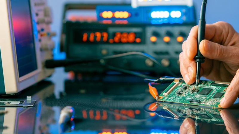
In-circuit testing (ICT) verifies the functionality and integrity of electronic components on a printed circuit board (PCB). In the manufacturing process of PCBs, components are mounted and soldered onto the board, creating a complex network of connections. Ensuring that each component and connection functions correctly is critical to the reliability of the final product.
ICT employs specialized test equipment that applies electrical probes to various points on the PCB, measuring parameters such as resistance, capacitance, and signal integrity. This process ensures each component operates within specified limits, detecting issues such as short circuits, open circuits, incorrect component values, and faulty solder joints.
The Inception of Electrical Testing
The evolution of ICT dates back to the early days of electronics manufacturing when manual inspection was the norm. As circuit complexity increased, automated ICT systems were developed, allowing for faster and more accurate testing. Today, ICT systems are integral to modern electronics manufacturing, providing high fault coverage and precision.
Common faults detected by ICT include solder bridges, missing components, and incorrect orientation of components. Unlike functional testing, which assesses the overall operation of a device, ICT provides a granular level of detail by examining each electronic and electrical component in isolation. This comprehensive approach ensures that faults are pinpointed accurately, making it easier to promptly address and rectify issues.
Compared to other testing methods, such as functional testing and visual inspection, ICT offers distinct advantages. It provides a higher level of fault coverage and precision, making it indispensable in ensuring product reliability and quality control.
Key Components of ICT
In-circuit testing relies on several essential components to ensure accurate and efficient testing of electronic circuits. Each component plays a vital role in the overall testing process, contributing to the precision and reliability of the results.
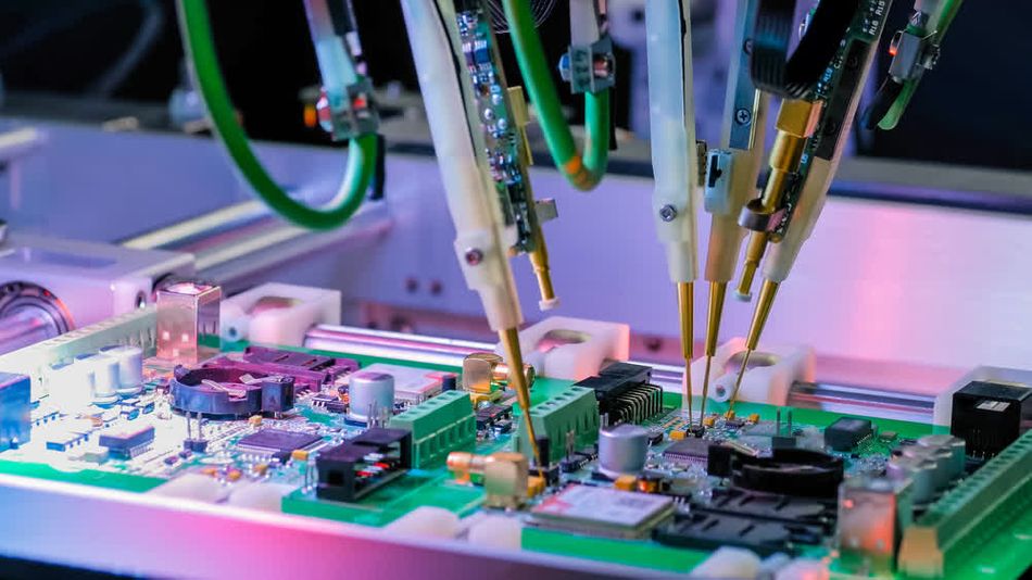
Test Fixtures - These are custom-designed holders that securely position the PCB for testing. They ensure that the test probes make proper contact with the test points on the PCB, providing stability and consistency during the testing process.
Test Probes - Test probes are fine, needle-like conductors that make electrical contact with specific points on the PCB. They measure various electrical parameters, such as voltage, current, resistance, and capacitance, to verify the functionality of each component.
Measurement Instruments - These devices include digital multimeters, oscilloscopes, and spectrum analyzers, which are used to measure and analyze the electrical signals on the PCB. They provide precise readings that are crucial for detecting faults and ensuring component performance.
Signal Generators - Signal generators produce specific electrical signals that are injected into the circuit during testing. These signals simulate the operating conditions of the circuit, allowing for comprehensive testing of the PCB's response to different inputs.
Switching Matrices - Switching matrices are used to route signals from the test instruments to the appropriate test points on the PCB. They enable the sequential testing of multiple test points without the need for manual intervention, increasing the efficiency and speed of the testing process.
Software and Control Systems - Advanced software and control systems manage the ICT process, from controlling the test equipment to analyzing the test results. These systems provide automated test routines, data logging, and real-time analysis, ensuring a thorough and efficient testing process.
How In-Circuit Testing Works
In-circuit testing (ICT) involves a series of meticulous steps designed to ensure the functionality and integrity of electronic components on a PCB. This process is integral to the quality assurance of electronic products, catching faults early in the manufacturing process and ensuring that each unit meets stringent performance standards.
Setting Up Test Fixtures
The PCB, a complex assembly of various electronic components and connections, is placed into a custom-designed test fixture. This fixture holds the PCB securely, ensuring accurate alignment and contact between the test probes and the PCB test points. Proper alignment is crucial as it directly impacts the accuracy of the measurements.
Program Loading
The test program, which contains the specific test sequences and parameters for the PCB under test, is loaded into the ICT system. This program is developed based on the PCB's design and expected performance characteristics, tailored to test each component and connection according to its specifications.
Power Supply
Power is applied to the PCB to simulate its operational state. This involves providing the necessary voltages and currents that the circuit would experience during normal operation. By doing so, the ICT system can accurately assess the functionality of the components under real-world conditions.
Electrical Connection Testing
The test probes make contact with various test points on the PCB to measure continuity and connectivity. This step ensures that all connections are correctly made and that there are no open circuits, which could lead to malfunction or failure of the device in actual use.
Component Verification
Each component on the PCB is tested individually. This involves measuring electrical parameters such as resistance, capacitance, and inductance to verify that each component meets its specified values.
Functional Testing
Functional tests are conducted to ensure that the PCB performs its intended functions. This may include checking signal paths, verifying the operation of integrated circuits, and ensuring that output signals are correct. By simulating real operating conditions, functional testing validates the overall performance of the PCB.
Data Collection and Analysis
During testing, data is collected from the various measurements and tests performed. This data is analyzed in real time to identify any discrepancies or faults. Advanced software tools automate this analysis, providing immediate feedback and allowing engineers to quickly pinpoint and address issues.
Fault Diagnosis and Reporting
If any faults are detected, the ICT system provides detailed diagnostic information. This includes the location of the fault, the nature of the defect, and possible causes. Such detailed reporting is essential for efficient troubleshooting and repair.
Re-testing After Repair
Once identified faults are repaired, the PCB undergoes re-testing to ensure that all issues have been resolved. This step verifies that the repairs were successful and that the PCB now meets all specifications, thus preventing recurring issues.
Final Quality Check
A final quality check is performed to confirm that the PCB is fully functional and free of defects. This comprehensive check ensures that the PCB is ready for use in its intended application, upholding the standards of reliability and performance expected in high-quality electronic products.
Difference Between ICT and Other Testing Methods
While in-circuit testing may seem identical to various other electrical testing methods, there are several significant and minor differences as shown in the following table:
Aspect | In-Circuit Testing (ICT) | Functional Testing | Boundary Scan Testing |
Purpose | Tests individual components in isolation | Tests overall functionality of the device | Tests interconnections and board-level functionality |
Fault Coverage | High for specific components | General, covers end-to-end functionality | High for interconnections |
Detail Level | Granular, component-specific | Broad, device-specific | Specific to interconnections |
Speed | Moderate, depending on the complexity of the PCB | Typically faster | Moderate to fast |
Implementation Cost | High, due to specialized fixtures and probes | Moderate to high | Moderate, depends on JTAG infrastructure |
Best Use Case | Early-stage manufacturing and quality control | Final product testing | Testing complex digital circuits |
Common Types of ICT Testers
There are several types of ICT testers depending on the type of tests required for PCBs. Here is a quick look:
Standard ICT - A traditional in-circuit tester (ICT) system uses fixed pin probes to contact test points on the printed circuit board (PCB) to check for defects.
Flying Probe Tester - This type of tester uses movable probes that can access components without needing fixed test points. It provides greater flexibility and test access but at a higher cost.
Suggested Reading: Flying Probe Test: An Extensive Guide to the Technology and Applications
Manufacturing Defect Analyzer (MDA) - An MDA employs non-contact probing to detect manufacturing and design defects using electromagnetic sensors. It checks for issues such as incorrect components, soldering defects, and track/land faults.
Cableform Tester - Used for flexible or rigid-flex PCBs. It features motorized probes to access both sides of the PCB and check for defects specific to flex circuits, such as conductor exposure or breaks.
Advantages of In-Circuit Testing
Speed and Accuracy
In-circuit testing (ICT) is renowned for its fast and accurate detection of component defects, continuity issues, and other faults. The efficiency of ICT allows for quick identification of problems, which is essential in maintaining high-quality production standards.
User-Friendly Operation
The operation of ICT is straightforward and user-friendly, significantly reducing the likelihood of operator errors. This simplicity contributes to a more reliable testing process.
Efficiency in High-Volume Production
With a testing time of usually 1-2 minutes per assembly, ICT is particularly well-suited for high-volume production environments. This rapid testing capability makes it an ideal choice for large-scale manufacturing operations.
Comprehensive Fault Coverage
ICT programming offers comprehensive and reliable testing methods that provide high fault coverage for manufacturing defects. This thorough approach ensures that a wide range of potential issues are detected and addressed.
Flexibility in Test Procedure Updates
The test procedure in ICT can be easily updated and modified, making it adaptable to various PCB designs and technologies. This flexibility ensures that ICT remains relevant and effective across different production requirements.
Disadvantages of In-Circuit Testing
High Fixture Costs
In-circuit test fixtures can be expensive to create and develop, particularly for low-volume production runs. This high initial cost can be a significant barrier for smaller production scales.
Challenges with High-Density SMT Components
For high-density, small package size surface-mount technology (SMT) components, ICT may not always identify connector faults effectively. The limitations in handling such components can restrict the use of ICT in certain applications.
Recommended Reading: SMT Manufacturing: Everything You Need to Know
Importance of Proper Contact
Achieving proper contact between the test pins and corresponding test pads is crucial for obtaining consistent results. Inconsistent contact can lead to unreliable test outcomes, necessitating careful maintenance and setup.
Maintenance of Test Pins
Failing to clean or replace test pins regularly can result in failures and false calls. This neglect can compromise the accuracy of the testing process, highlighting the need for regular maintenance.
Time-Consuming Test Program Creation
Creating ICT test programs can be a time-consuming process, especially for intricate PCB designs. The effort required for test program development can add to the overall production timeline.
Technological Advancements in In-Circuit Testing
Enhanced Test Capabilities
The evolution of ICT technology has been driven by the increasing complexity of electronic devices, which demand more precise and efficient testing methods.
High Precision Test Probes - These probes can make extremely fine contact with tiny test points on modern PCBs, which are becoming increasingly dense with components. The precision of these probes ensures accurate measurement of electrical parameters, reducing the likelihood of false readings and improving fault detection accuracy. This development is crucial as PCBs in devices like smartphones and wearables become smaller and more complex.
ML-Powered Advanced Algorithms - These algorithms analyze vast amounts of data collected during testing to identify patterns and anomalies that indicate potential faults. Furthermore, machine learning techniques enhance this analysis by enabling predictive maintenance and early fault detection before they cause significant issues. For example, algorithms can now detect subtle changes in component behavior that may indicate a future failure, allowing for proactive maintenance.
Recommended Reading: Harnessing AI Platforms for Rapid Development and Deployment of Predictive Maintenance Systems in Industrial Applications.
Automated Optical Inspection - AOI systems use high-resolution cameras to visually inspect PCBs for defects such as solder bridges and missing components. When combined with ICT, AOI provides a comprehensive testing solution that covers both electrical and visual inspection, ensuring thorough fault detection. This integration is particularly beneficial for speed-critical high-volume production.

- Multi-Site Testing - Multi-site testing allows multiple PCBs to be tested simultaneously, significantly reducing the time required for testing large batches of PCBs. The ability to test several units at once without compromising accuracy means that manufacturers can meet tight production schedules without sacrificing quality.
Further Reading: PCB Panelization: Everything You Need to Know
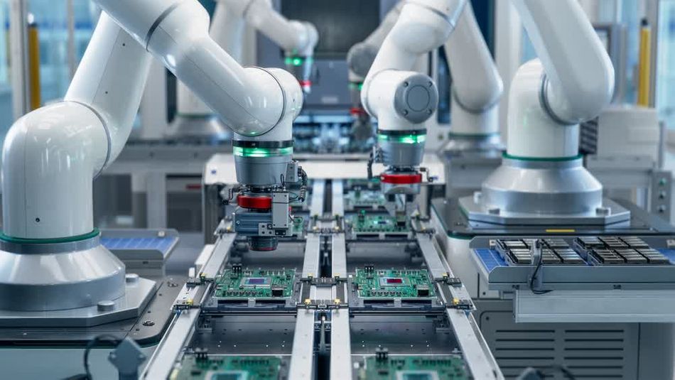
Integration with Automation
In-circuit testing (ICT) is increasingly being integrated with advanced automation systems, enhancing the efficiency and accuracy of the testing process. This integration leverages specific technologies and communication protocols to streamline operations and minimize human intervention.
Programmable Logic Controllers - PLCs can control and automate the testing sequences, ensuring precise timing and coordination of the test steps. By programming these controllers, manufacturers can automate the repetitive aspects of ICT, reducing the potential for human error and increasing throughput.
Robotics Arms - Robotic systems can handle PCBs with high precision, positioning them accurately within test fixtures and moving them through various stages of the testing process. The process speeds up the testing process and ensures consistent handling of delicate PCBs, preventing damage that might occur with manual handling.
Advanced Communication Systems - Specific communication protocols, such as Modbus and OPC UA (Open Platform Communications Unified Architecture), facilitate seamless communication between ICT equipment and automated systems. These protocols enable real-time data exchange and coordination, allowing different components of the automation system to work in harmony.
Advantages of Automating In-Circuit Testing Systems
The benefits of integrating ICT with automation systems are numerous:
Increased Efficiency:
Automated systems can operate continuously without fatigue, leading to higher productivity and faster turnaround times.
PLCs and robotic arms can execute test sequences more rapidly than manual operations, significantly reducing the time required for testing large batches of PCBs.
Reduced Human Error:
Automation minimizes the potential for human mistakes, such as incorrect probe placement or inconsistent handling of PCBs.
Automated data logging and analysis ensure accurate record-keeping and immediate identification of issues.
Consistent Quality:
Robotic handling ensures that each PCB is tested under identical conditions, leading to more consistent and reliable results.
Automated systems maintain precise control over test conditions, ensuring repeatability and accuracy.
Enhanced Data Management:
- Communication protocols like OPC UA facilitate the integration of ICT systems with enterprise resource planning (ERP) and manufacturing execution systems (MES), enabling comprehensive data management and traceability.
Real-time data exchange allows for immediate adjustments and optimization of the testing process based on collected data.
Software Innovations
The latest software developments in in-circuit testing (ICT) have significantly enhanced the capabilities and efficiency of testing processes. These innovations focus on advanced data analysis algorithms, remote monitoring capabilities, and user-friendly interfaces, transforming how engineers approach ICT.
Remote Monitoring Capabilities - It allows engineers to oversee testing processes via PLC and SCADA systems from anywhere in the world. This capability is particularly beneficial for large-scale manufacturing operations spread across multiple locations. Remote monitoring tools enable real-time data access and control, reducing downtime and improving response times to any issues that arise during testing. \
User-Friendly Interfaces - Modern ICT software is designed to simplify the testing process, making it accessible even to those with limited technical expertise. Features such as drag-and-drop test configuration, visual dashboards, and interactive reports help streamline workflows and reduce the learning curve.
Challenges and Considerations in In-Circuit Testing
Limitations of ICT
In-circuit testing (ICT) comes with several inherent technical limitations that can impact the testing process:
Limited Fault Coverage:
ICT can miss certain types of defects, such as those affecting circuit functionality under specific conditions that are not replicated during testing.
Impact - This limitation can lead to undetected faults progressing through the manufacturing process, potentially causing failures in the field.
Complex Test Fixture Design:
Designing and manufacturing test fixtures for ICT can be complex and time-consuming, especially for high-density PCBs.
Impact - This complexity increases setup times and can delay the overall testing process.
Dependency on Accurate Test Point Access:
ICT requires precise access to test points on the PCB, which can be challenging for miniaturized and densely packed boards.
Impact - Difficulty in accessing test points can lead to incomplete testing and reduced fault detection capabilities.
Sensitivity to PCB Variations:
Variations in PCB manufacturing, such as slight differences in component placement or solder joint quality, can affect the accuracy of ICT.
Impact - These variations can result in false positives or negatives, complicating the troubleshooting process.
Cost and Resource Implications
Cost is perhaps the biggest limitation of in-circuit testing. Implementing ICT involves various cost and resource considerations, which differ based on the scale of production. Below is an analysis of these factors:
Cost Factors | Small-Scale Production | Large-Scale Production |
Initial Setup Costs | High per unit | Lower per unit |
Operational Costs | High per unit | Lower per unit |
Economies of Scale | Limited | Significant |
Maintenance & Calibration | High relative cost | Lower relative cost |
Rework & Scrap Rates | Potentially higher | Reduced due to better detection |
Overcoming Common Issues
Here are strategies for overcoming common issues faced in ICT, with technical methods and tools:
Enhancing Fault Coverage:
Method: Implement complementary testing methods, such as functional testing and boundary scan testing.
Tools: Use automated test equipment (ATE) that supports multiple testing techniques.
Simplifying Test Fixture Design:
Method: Employ modular test fixtures that can be easily adapted for different PCB designs.
Tools: Utilize computer-aided design (CAD) software to streamline the fixture design process.
Improving Test Point Access:
Method: Design PCBs with dedicated test access points to facilitate easier probing.
Tools: Use high-density interconnect (HDI) technology to create accessible test points without compromising board space.
Mitigating PCB Variations:
Method: Implement tighter manufacturing tolerances and quality control processes to reduce variations.
Tools: Use statistical process control (SPC) software to monitor and control manufacturing processes.
Reducing False Positives/Negatives:
Method: Calibrate ICT equipment regularly and use reference boards to validate test accuracy.
Tools: Employ precision measurement tools and calibration standards.
By addressing these challenges with targeted strategies and advanced tools, the effectiveness and reliability of ICT can be significantly enhanced, ensuring higher quality in electronic manufacturing.
Conclusion
In-circuit testing (ICT) is pivotal in ensuring the quality and reliability of electronic products. It provides a comprehensive approach to detecting and diagnosing faults at an early stage, preventing defective components from reaching the market. Through advancements in test capabilities, integration with automation, and innovative software solutions, ICT has become an indispensable tool in modern engineering.
ICT's ability to provide detailed fault coverage, coupled with its integration into automated systems, significantly enhances manufacturing efficiency and product quality. As electronic devices continue to evolve, the role of ICT will expand further, incorporating more sophisticated testing methodologies and integrating with advanced technologies such as AI and machine learning. This evolution will drive even greater precision in fault detection and maintenance, securing ICT's position as a cornerstone of quality assurance in engineering.
Frequently Asked Questions
What types of faults can ICT detect?
Short Circuits: ICT can identify unintended connections between two points in a circuit, which can cause excessive current flow and damage components.
Open Circuits: ICT detects breaks in the circuit path, preventing current from flowing as intended.
Incorrect Component Values: ICT verifies that components such as resistors and capacitors have the correct values specified in the design.
Misaligned or Missing Components: ICT checks for components that are incorrectly placed or missing from the PCB.
Solder Bridges: ICT identifies unwanted solder connections between conductive traces, which can lead to short circuits.
Functional Failures: ICT tests individual components and their functionality within the circuit to ensure they operate correctly under specified conditions.
2. What are the typical costs associated with implementing ICT?
Implementing ICT involves several cost factors:
Initial Equipment Investment:
High upfront costs for test equipment and fixtures.
Custom test fixtures designed for specific PCB layouts.
Maintenance and Calibration:
Ongoing costs for maintaining and calibrating test equipment to ensure accuracy.
Regular updates to software and hardware components.
Training and Labor:
Training personnel to operate and maintain ICT systems.
Skilled labor required to design and implement test strategies.
Production Scale:
Costs vary significantly between small-scale and large-scale production.
Economies of scale can reduce per-unit testing costs in large-scale operations.
Development and Setup Time:
Time required to develop test programs and set up ICT equipment.
Initial setup time can be substantial, impacting overall project timelines.
3. What types of defects can ICT detect?
ICT can detect various defects including shorts, opens, incorrect component values, missing components, and incorrect component placement. It can also test for functional aspects such as signal integrity and circuit performance under certain conditions.
4. How does ICT differ from functional testing?
ICT focuses on the individual components and connections on the PCB, ensuring that each component is correctly placed and functioning properly. Functional testing, on the other hand, tests the PCB as a whole unit to ensure it performs its intended functions in a real-world scenario. ICT is typically done before functional testing.
5. What equipment is used for ICT?
ICT equipment includes test fixtures (also known as bed-of-nails fixtures), a test system with a computer to control the testing process, and software to manage and analyze the test results. The fixtures have probes that make contact with test points on the PCB.
6. What are the benefits of using ICT?
ICT provides several benefits including early detection of manufacturing defects, reducing the cost and time of rework, ensuring high-quality assembly, and increasing the overall reliability of the final product. It is a highly efficient and accurate method for quality control in PCB manufacturing.
References
Table of Contents
IntroductionUnderstanding In-Circuit Testing: The BasicsWhat is In-Circuit Testing (ICT)?The Inception of Electrical TestingKey Components of ICTHow In-Circuit Testing WorksSetting Up Test FixturesProgram LoadingPower SupplyElectrical Connection TestingComponent VerificationFunctional Testing Data Collection and AnalysisFault Diagnosis and ReportingRe-testing After RepairFinal Quality CheckDifference Between ICT and Other Testing MethodsCommon Types of ICT TestersAdvantages of In-Circuit TestingSpeed and Accuracy User-Friendly Operation Efficiency in High-Volume ProductionComprehensive Fault Coverage Flexibility in Test Procedure Updates Disadvantages of In-Circuit TestingHigh Fixture Costs Challenges with High-Density SMT Components Importance of Proper Contact Maintenance of Test Pins Time-Consuming Test Program Creation Technological Advancements in In-Circuit TestingEnhanced Test CapabilitiesIntegration with AutomationAdvantages of Automating In-Circuit Testing SystemsSoftware InnovationsChallenges and Considerations in In-Circuit TestingLimitations of ICTCost and Resource ImplicationsOvercoming Common IssuesConclusionFrequently Asked Questions2. What are the typical costs associated with implementing ICT?3. What types of defects can ICT detect?4. How does ICT differ from functional testing?5. What equipment is used for ICT?6. What are the benefits of using ICT?References